Semiconductor device

a semiconductor device and semiconductor technology, applied in the field of semiconductor devices for electrostatic protection, can solve the problems of reducing the packing density of the semiconductor device, the conventional techniques described above, etc., and achieve the effects of stable semiconductor device, reduced chip area, and low cos

Inactive Publication Date: 2007-04-10
PANASONIC CORP
View PDF4 Cites 25 Cited by
  • Summary
  • Abstract
  • Description
  • Claims
  • Application Information

AI Technical Summary

Benefits of technology

[0039]Thus, the chip area increases by an amount corresponding to the third island region, which reduces the packing density of the semiconductor device.
[0102]As is apparent from the above, a stable semiconductor device can be provided at low cost.

Problems solved by technology

The conventional techniques described above, however, have the following problems.
This may decrease the packing density of the semiconductor device.

Method used


Image

  • Semiconductor device
  • Semiconductor device
  • Semiconductor device

Examples


first embodiment

(First Embodiment)

[0115]Hereinafter, a semiconductor device according to a first embodiment of the present invention will be described with reference to the accompanying drawings.

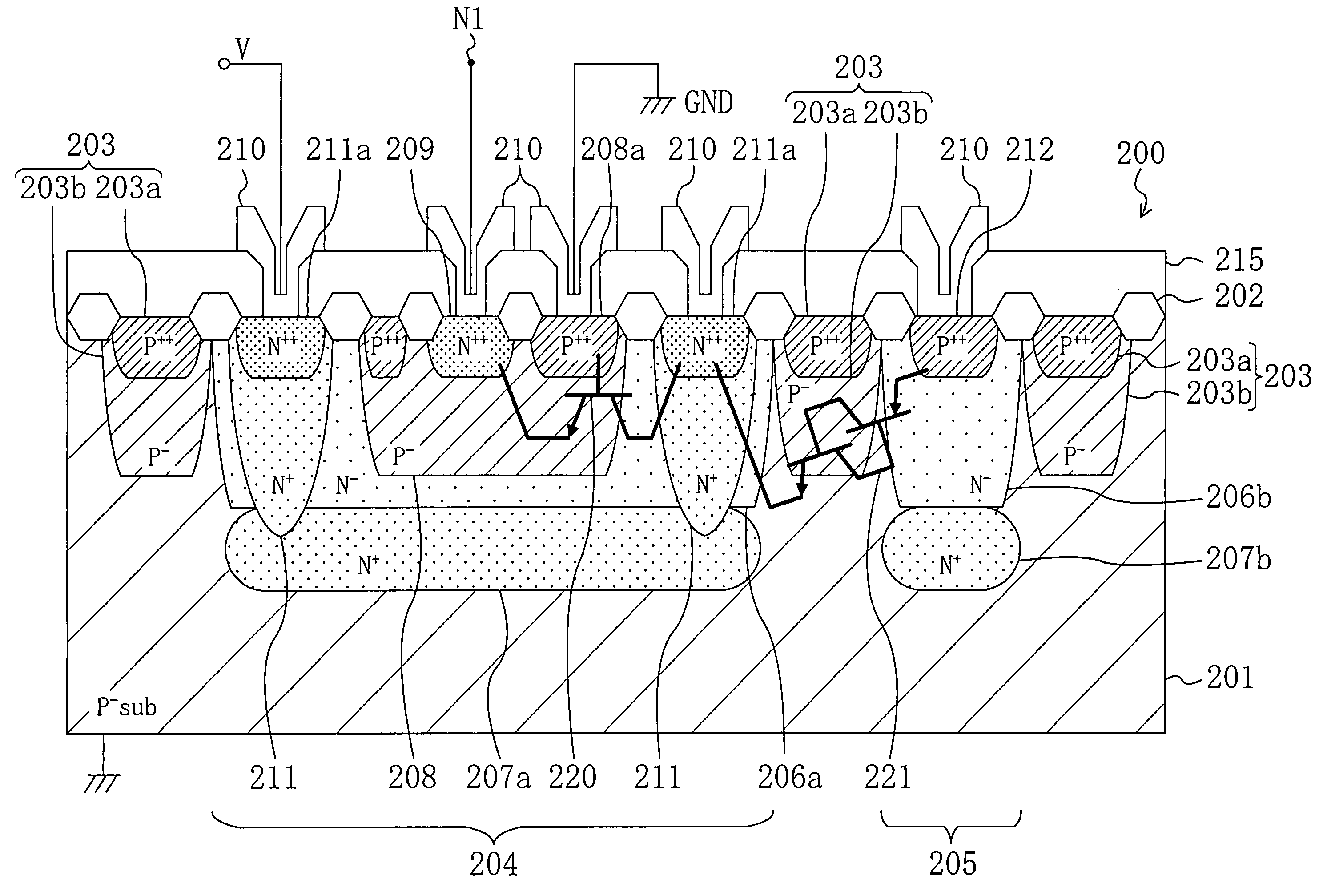
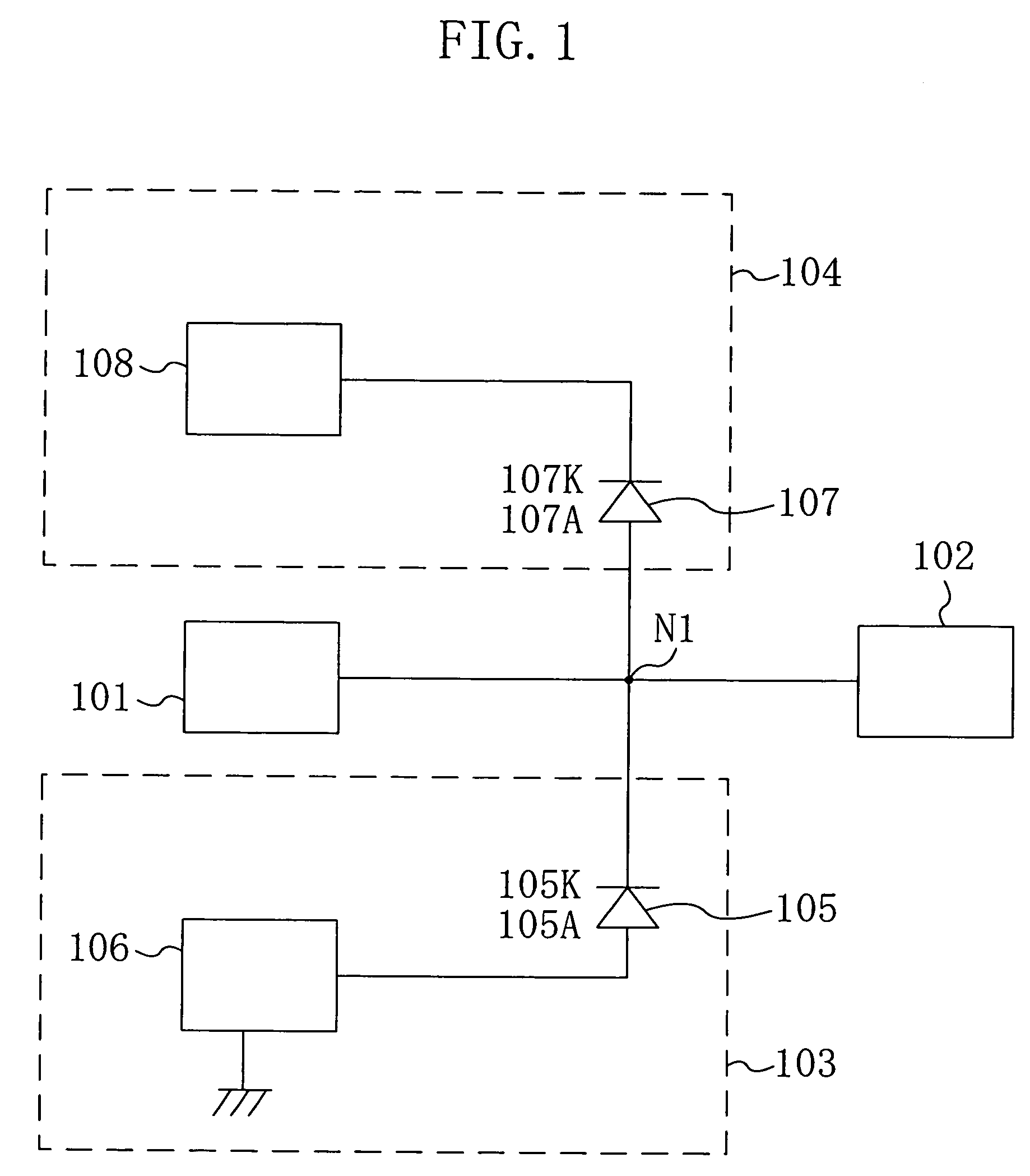
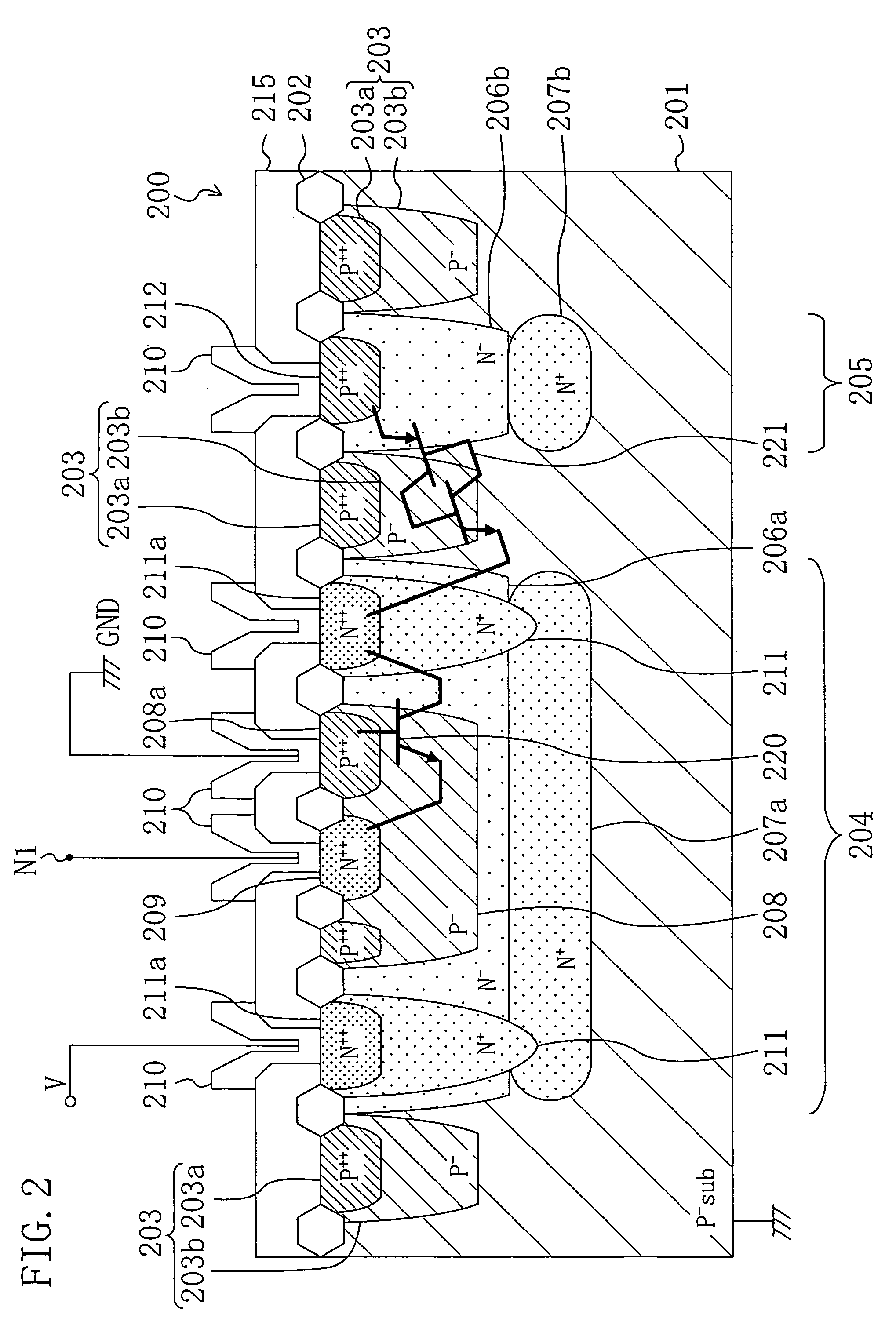
[0116]FIG. 1 is an equivalent circuit diagram of circuitry configured in the semiconductor device according to the first embodiment. The semiconductor device includes an output pad 101 electrically connected to an inductive load (not shown), and a driver element 102 electrically connected to the output pad 101 and supplying a current. At a connecting point N1 positioned between the output pad 101 and the driver element 102, a negative surge absorbing unit 103 and a positive surge absorbing unit 104 are electrically connected to each other.

[0117]In this device, the negative surge absorbing unit 103 is provided with a negative surge protection diode 105 and a GND terminal 106. The negative surge protection diode 105 has a cathode 105K electrically connected to the connecting point N1 and an anode 105A electri...

second embodiment

(Second Embodiment)

[0157]Next, a semiconductor device according to a second embodiment of the present invention will be described with reference to the accompanying drawings.

[0158]Also in the second embodiment, circuitry corresponding to the equivalent circuit diagram shown in FIG. 1 is configured. The second embodiment differs from the first embodiment in the structure of the negative surge absorbing unit 104. Hence, this difference will be described in detail.

[0159]FIG. 4 is a view showing a cross section of a semiconductor device 200a according to the second embodiment. The illustrated semiconductor device 200a has the structure in which several components are added to the semiconductor device 200 of the first embodiment shown in the sectional view of FIG. 2. Thus, description of the components of the semiconductor device 200a shown in FIG. 4 that are the same as those of the semiconductor device 200 shown in FIG. 2 will be omitted by retaining the same reference numerals, and th...

third embodiment

(Third Embodiment)

[0175]Next, a semiconductor device according to a third embodiment of the present invention will be described with reference to the accompanying drawings.

[0176]Also in the third embodiment, circuitry corresponding to the equivalent circuit diagram shown in FIG. 1 is configured. The third embodiment differs from the first and second embodiments in the structure of the negative surge absorbing unit 104. Hence, this difference will be described in detail.

[0177]FIG. 5 is a sectional view of a semiconductor device 200a according to the third embodiment. The semiconductor device 200a contains the structure in common with the semiconductor device 200 of the first embodiment, so that in the third embodiment, the difference between the semiconductor devices 200a and 200 will be mainly described.

[0178]Note that the plane structure of the semiconductor device 200a is similar to that shown in FIG. 3.

[0179]In the semiconductor device 200 of the first embodiment, the n-wells (in...


PUM


Abstract

A semiconductor device includes an output pad and a surge absorption unit formed above a semiconductor region of a first conductivity type. The surge absorption unit includes: a semiconductor island region of a second conductivity type; a buried layer of the second conductivity type formed between a bottom of the semiconductor island region of the second conductivity type and the semiconductor region of the first conductivity type; a dopant layer of the first conductivity type formed in an upper portion of the semiconductor island region of the second conductivity type and connected to have the same potential as the semiconductor region of the first conductivity type; a dopant layer of the second conductivity type formed in an upper portion of the dopant layer of the first conductivity type and electrically connected to the output pad; and a ring layer of the second conductivity type surrounding the dopant layer of the first conductivity type and reaching the buried layer of the second conductivity type. In this device, the ring layer of the second conductivity type is electrically connected to a terminal with a fixed potential and contains a dopant of the second conductivity type having a higher concentration than the semiconductor island region of the second conductivity type.

Description

CROSS-REFERENCE TO RELATED APPLICATIONS[0001]This application claims priority under 35 U.S.C. § 119 on Patent Application No. 2004-121339 filed in Japan on Apr. 16, 2004, the entire contents of which are hereby incorporated by reference.BACKGROUND OF THE INVENTION[0002](a) Fields of the Invention[0003]The present invention relates to semiconductor devices, and in particular to electrostatic protection semiconductor devices capable of protecting their internal elements against breakdown due to an electrostatic surge or the like.[0004](b) Description of Related Art[0005]Recently, with increasing packing density and decreasing power consumption of a semiconductor integrated circuit device, a driver for driving an inductive load has also been requested to increase the packing density and decrease the power consumption.[0006]Herein, the inductive load is a load to which a voltage is applied from outside to pass a current and to generate an induced voltage having a polarity opposite to th...

Claims


Application Information

Patent Timeline
Patent Type & Authority Patents(United States)
IPC IPC(8): H01L23/62H01L23/60H01L27/02H01L27/04H01L29/76
CPCH01L27/0262H01L2924/0002H01L2924/00
Inventor IMAHASHI, MANABUOGURA, HIROYOSHINAWATE, MASAKATSU
Owner PANASONIC CORP
Why Eureka
Try Eureka