Oscillator circuit and L load differential circuit achieving a wide oscillation frequency range and low phase noise characteristics

a technology of oscillator circuit and load differential circuit, which is applied in the direction of oscillator generator, pulse technique, instruments, etc., can solve the problems of reducing yield, difficult to achieve a wide oscillation frequency range, and reducing yield, so as to prevent deterioration of phase noise characteristics, wide oscillation frequency range, and low phase noise

Inactive Publication Date: 2007-04-10
RENESAS ELECTRONICS CORP
View PDF17 Cites 27 Cited by
  • Summary
  • Abstract
  • Description
  • Claims
  • Application Information

AI Technical Summary

Benefits of technology

[0027]According to the invention described above, since the oscillation frequency of the oscillator circuit is controlled by varying the inductance of the LC resonant circuit, it is possible to achieve the oscillator circuit, which can prevent deterioration of the phase noise characteristics in a low oscillation frequency range, and can achieve a wide oscillation frequency range and characteristics ensuring low phase noises.
[0028]Further, the two inductance-variable portions included in the differential LC resonant circuit are electrically coupled to form an inductor pair by the switch circuit arranged between the inductance-variable portions. Thereby, it is possible to suppress deterioration of a Q value of the resonant circuit, and the voltage control oscillator circuit can have characteristics ensuring low phase noises. If the differential LC resonant circuit is configured not to connect a capacitor element thereto, it can be used as an L load differential circuit having a high Q value and a variable inductance.

Problems solved by technology

Meanwhile, the transistor elements formed on the same substrate do not necessarily exhibit designed characteristics due to variations in manufacturing steps.
Therefore, inductance mismatching occurs between the inductor elements, which reduces yield.
Accordingly, it is difficult to achieve a wide oscillation frequency range.
In a low frequency range, therefore, oscillation amplitude Aosc is low, and a signal-to-noise ratio of the oscillation signal is low so that the phase noise characteristics are impaired.
The foregoing inductance-variable element suffers from such a problem that the Q value lowers due to an on-resistance of a switch circuit connected in series to the inductor element.
This results in deterioration of the phase noise characteristics of the oscillator circuit formed of the inductor element.

Method used


Image

  • Oscillator circuit and L load differential circuit achieving a wide oscillation frequency range and low phase noise characteristics
  • Oscillator circuit and L load differential circuit achieving a wide oscillation frequency range and low phase noise characteristics
  • Oscillator circuit and L load differential circuit achieving a wide oscillation frequency range and low phase noise characteristics

Examples


first embodiment

[0045][First Embodiment]

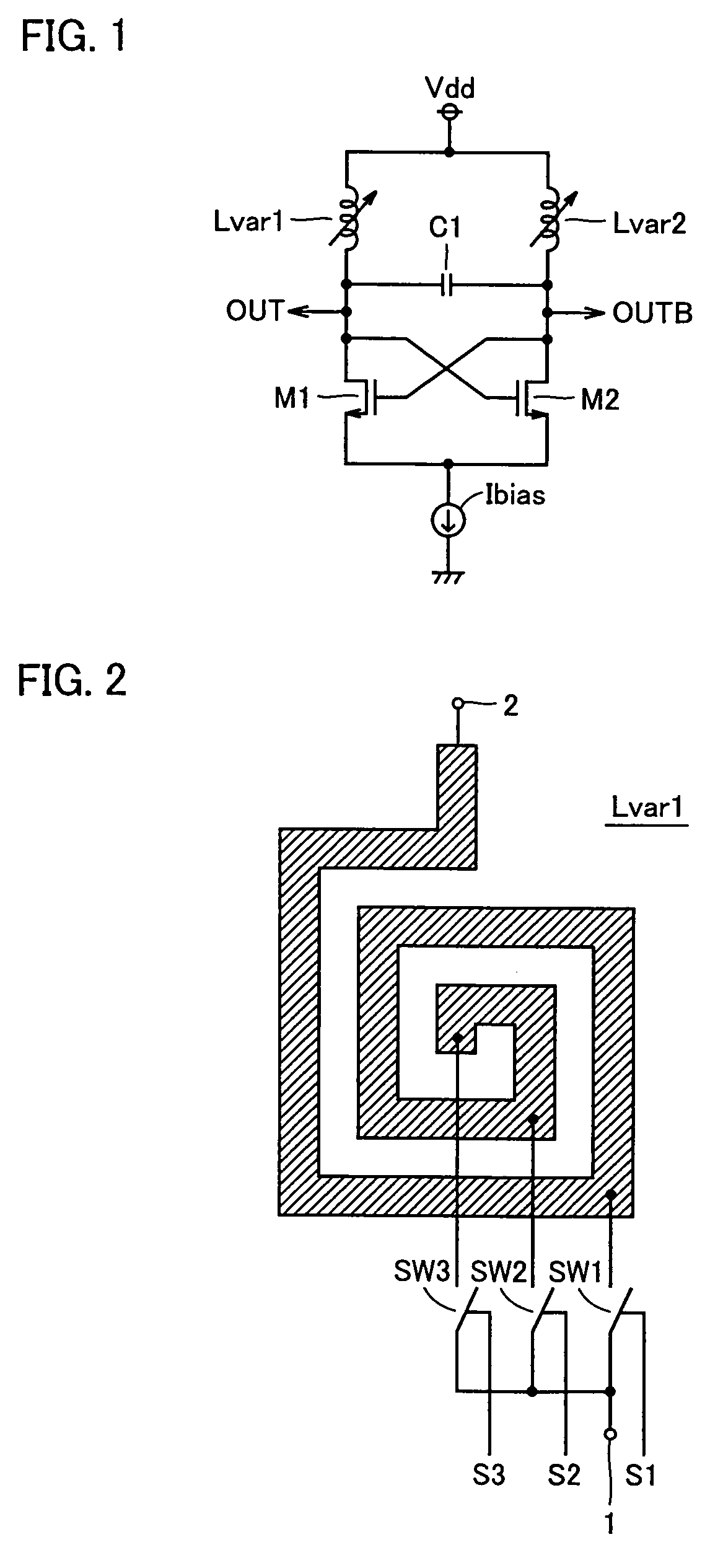
[0046]FIG. 1 shows a structure of an oscillator circuit according to a first embodiment of the invention. In the following description of the embodiment, a voltage control oscillator circuit will be described as an example of the oscillator circuit.

[0047]Referring to FIG. 1, a voltage control oscillator circuit is formed of a differential type LC resonant circuit, which is formed of inductance-variable portions Lvar1 and Lvar2 having variable inductances and a capacitor element C1, and a positive feedback circuit formed of N-channel MOS transistors M1 and M2.

[0048]Each of inductance-variable portions Lvar1 and Lvar2 has first and second input / output terminals, and the second input / output terminal is commonly connected to an external power supply node Vdd. The first input / output terminals are connected to output nodes OUT and OUTB, respectively. Capacitor element C1 is connected between the first input / output terminals of inductance-variable portions Lvar1 and...

second embodiment

[0103][Second Embodiment]

[0104]FIG. 10 shows by way of example an oscillator circuit according to a second embodiment of the invention. Similarly to the first embodiment, a voltage control oscillator circuit will be described as an example of the oscillator circuit.

[0105]Referring to FIG. 10, the voltage control oscillator circuit differs from the voltage control oscillator circuit shown in FIG. 1 only in that the capacitor element forming the LC resonant circuit has a variable capacitance. Description of the same or corresponding portions is not repeated.

[0106]The LC resonant circuit is formed of inductance-variable portions Lvar1 and Lvar2 each connected between external power supply node Vdd and output node OUT or OUTB, and a variable capacitor element Cvar connected between first input / output terminals of inductor elements Lvar1 and Lvar2. In the following description, it is assumed that each passive element has an inductance of L and a capacitance value of C.

[0107]In this struc...

third embodiment

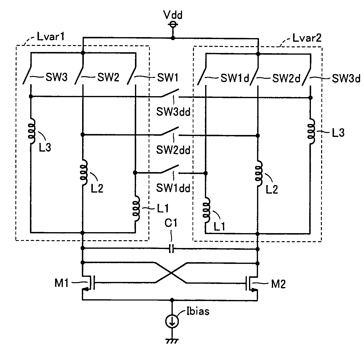
[0112][Third Embodiment]

[0113]FIG. 11 shows a structure of an oscillator circuit according to a third embodiment of the invention. A voltage control oscillator circuit will now be described as an example of an oscillator circuit.

[0114]Referring to FIG. 11, the voltage control oscillator circuit includes switch circuits SW1dd–SW3dd arranged between inductance-variable portions Lvar1 and Lvar2 of the differential LC resonant circuit, in addition to the components of the voltage control oscillator circuit of the first embodiment shown in FIG. 5. Description of the same or corresponding portions is not repeated.

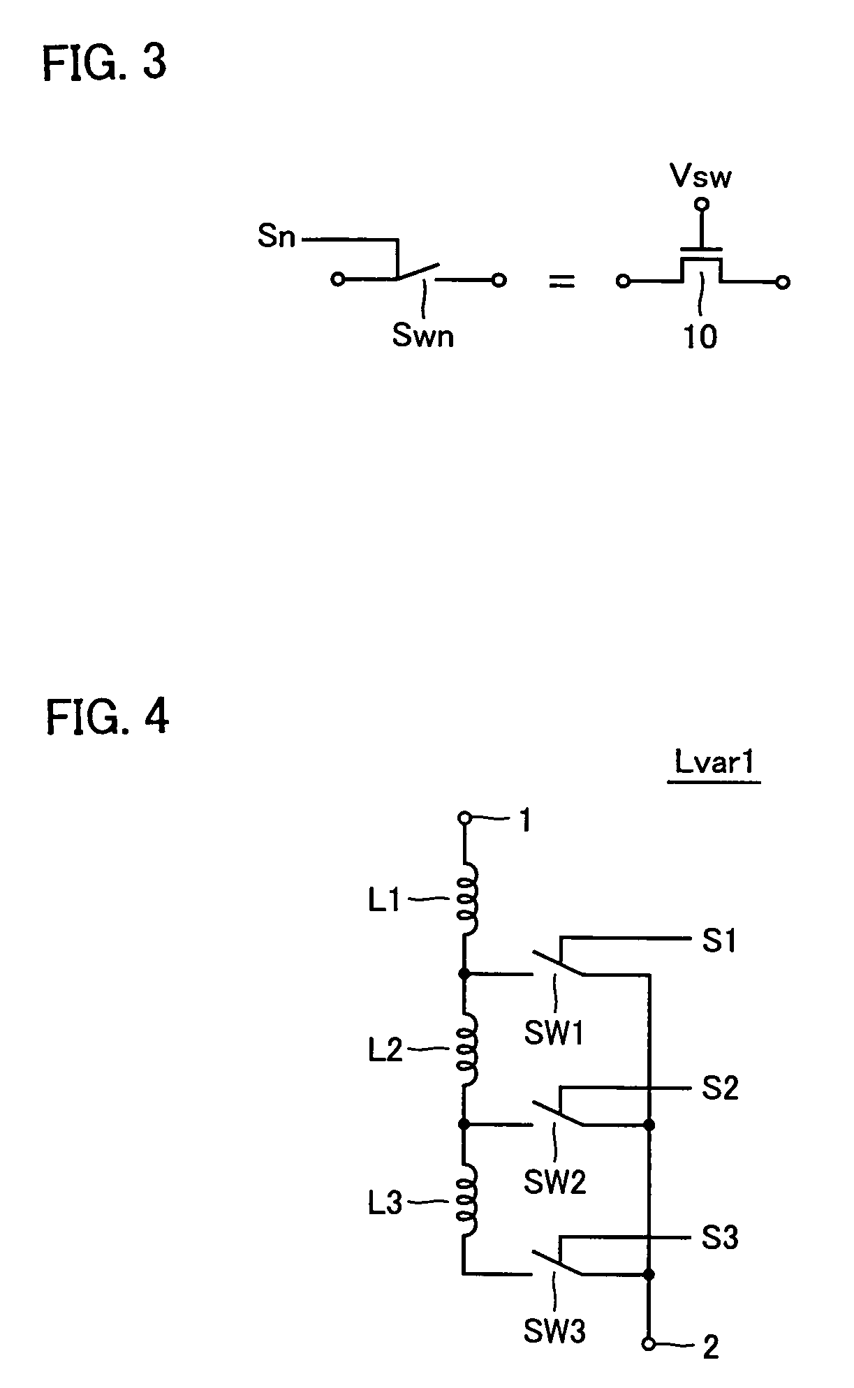
[0115]Inductance-variable portions Lvar1 and Lvar2 include switch circuits SW1–SW3 or SW1d–SW3d arranged corresponding to the respective turns, similarly to inductance-variable portion Lvar1 shown in FIG. 2.

[0116]Further, a switch circuit SW1dd is arranged between switch circuits SW1 and SW1d. A switch circuit SW2dd is arranged between switch circuits SW2 and SW2d. A switch circu...


PUM


Abstract

An oscillator circuit is formed of a differential LC resonant circuit formed of an L load differential circuit including inductance-variable portions and a capacitive element, and a positive feedback circuit formed of N-channel MOS transistors. The inductance-variable portion is configured to vary the inductance by selecting a plurality of switch circuits arranged between a plurality of arbitrary positions on a spiral interconnection layer and the input / output terminal, and thereby can control an oscillation frequency. The inductance-variable portions form an inductor pair when the switch circuit among the switch circuits coupled between the first input / output terminals is turned on together with the switch circuit.

Description

CROSS REFERENCE TO RELATED APPLICATIONS[0001]This application is a Division of U.S. application Ser. No. 10 / 644,865 filed on Aug. 21, 2003 now abandoned.BACKGROUND OF THE INVENTION[0002]1. Field of the Invention[0003]The present invention relates to an oscillator circuit and an L load differential circuit, and particularly to an oscillator circuit using an LC resonant circuit as well as an L load differential circuit mountable on the oscillator circuit.[0004]2. Description of the Background Art[0005]In wireless devices such as a cellular phone, a local oscillator circuit is used for frequency conversion of received signals into low-frequency signals allowing demodulation and for frequency conversion of send signals (i.e., signals to be sent) into high-frequency signals, and is required to have a wide oscillation frequency range and can lower noises (phase noises) at and around an oscillation frequency.[0006]A Voltage Control Oscillator (VCO), which is a kind of local oscillator circ...

Claims


Application Information

Patent Timeline
Patent Type & Authority Patents(United States)
IPC IPC(8): H03B5/18H03B5/08H03B5/12
CPCH03B5/1847H03B5/1228H03B5/1268H03B5/1256H03B5/1243H03B5/1265H03B5/1215H03B5/18
Inventor KOMURASAKI, HIROSHISANO, TOMOHIROSATO, HISAYASUKUMAMOTO, TOSHIOHASHIZUME, YASUSHI
Owner RENESAS ELECTRONICS CORP
Why Eureka
Try Eureka