Parallelism adjustment device

a technology of parallel adjustment and adjustment device, which is applied in the direction of photomechanical equipment, instruments, applications, etc., can solve the problems of inability to implement nano-scale features in mass production, inability to achieve mass production, and inability to achieve the effect of achieving high degree of freedom, instant responsiveness, and enhanced horizontal alignment in the imprinting process

Inactive Publication Date: 2007-04-17
IND TECH RES INST
View PDF8 Cites 55 Cited by
  • Summary
  • Abstract
  • Description
  • Claims
  • Application Information

AI Technical Summary

Benefits of technology

[0017]Furthermore, the parallelism adjustment mechanism includes a pressure sensor for sensing the applied pressure, so as to monitor the pressure instantly. With a pressure-time control curve previously established, the nano-imprinting process can be controlled. Meanwhile, the imprint unit and the carrier unit may be coupled to an alignment platform with a large area, so as to enhance the horizontal alignment in the imprinting process.
[0018]Accordingly, the parallelism adjustment device is proposed to achieve objectives such as high level of freedom, instant responsiveness, and no harm done to the mold and the substrate. After the imprint unit makes a contact with the carrier unit, non-uniform pressure distribution that occurs during the imprinting process is offset with the pressure exerted by the enclosed resilient membrane and the fluid. That is, when both the imprint unit and the carrier unit suffer from the poor parallelism, the parallelism may be adjusted passively via instant deformation of the resilient membrane, while such adjustment is can be made at wider angles without limited by the direction. With the property of the fluid, the pressure is evenly applied to the substrate of the carrier unit, in order to satisfy efficient and high quality imprinting requirements. And instead of placing in the closed chamber, the imprint unit and the carrier unit are operated independently, so complex preparations prior to the imprinting can be omitted. Accordingly, the present invention has a simple construction manufactured with a low cost, and the commercial demand is met for mass production at a rapid rate.

Problems solved by technology

As the demand for producing smaller line widths of integrated circuit increases, the use of conventional photolithography process to define line widths that are smaller than the wavelength of light for implementing nano-scale features becomes increasingly difficult due to the diffraction of light.
Although subnano-scale features have also been studied, they still cannot be implemented in mass production because the current commercially available manufacturing equipment is not compatible with the subnano-scale process.
Therefore, if the pressure distribution on the molding plates and the parallelism between the mold and the substrate are not adequately controlled, the imprinting precision is adversely affected, and the nano-scale features on the mold or even the substrate will be damaged.
The current processing apparatus does not meet the high requirements of nano-imprint lithography.
Therefore, the parallelism between the mold 63 and the substrate 64 is not ensured due to possible manufacturing errors or an improper assembly of components such as the mold and guide.
Furthermore, the oil hydraulic system has disadvantages such as poor control response.
The sealing and imprinting of this apparatus are complex and time-consuming, which is unfavorable to efficient mass production.
Furthermore, since the processing of the mold 82 and the substrate 83 requires stacking, sealing, transferring into the pressure chamber, and a pressure increasing and decreasing steps, it is difficult to achieve precision alignment due to the combined variability of all the processing steps.
This method is complex and requires generating high pressure, which consumes a lot of energy and may cause environmental pollution.

Method used


Image

  • Parallelism adjustment device
  • Parallelism adjustment device
  • Parallelism adjustment device

Examples


Embodiment Construction

[0028]Wherever possible in the following description, like reference numerals will refer to like elements and parts unless otherwise stated.

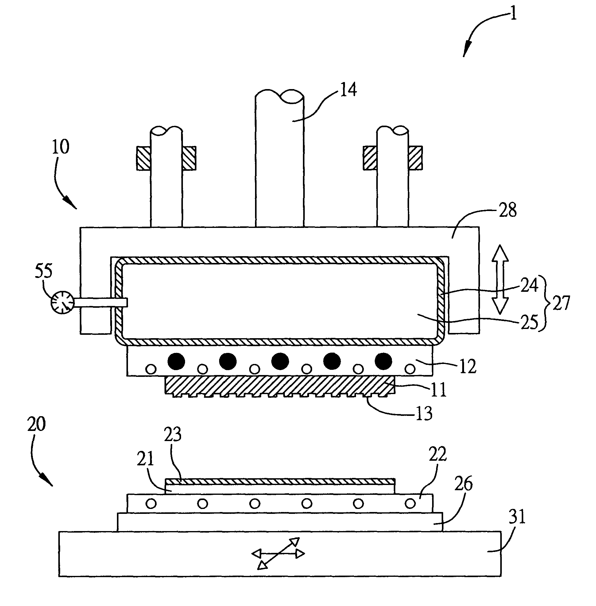
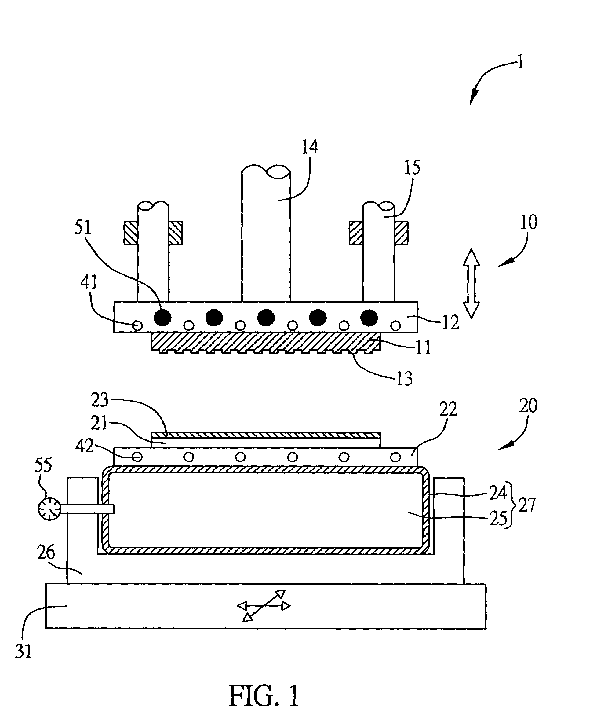
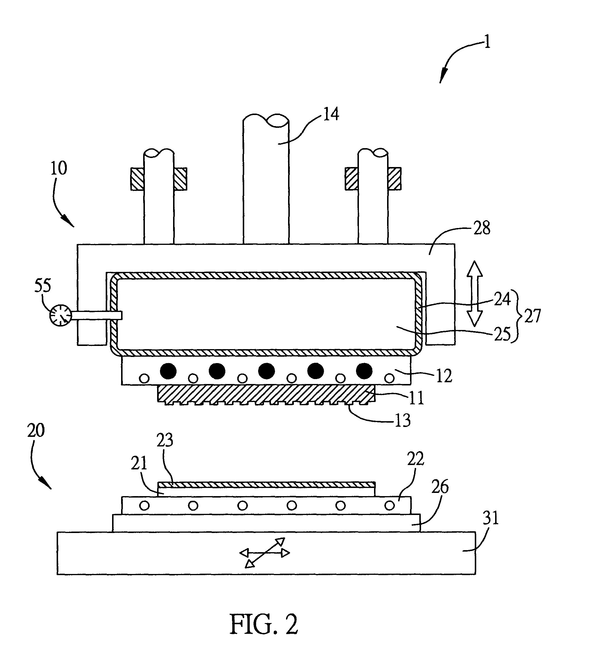
[0029]FIG. 1 depicts a parallelism adjustment device 1 applicable to nano-imprint lithography (NIL) according to the first embodiment of the invention. The parallelism adjustment device 1 includes an imprint unit 10 consisting of a mold 11, a first molding plate 12 and a driving source 14. The imprint unit 10 moves toward a carrier unit 20 by means of a plurality of the guiding poles 15. At least one nano-scale feature 13 to be imprinted is previously formed on the mold 11. The carrier unit 20 includes a second molding plate 26 mounted on a positioning platform 31. A resilient film 24 capable of withstanding high pressure is formed inside the second molding plate 26, and hermetically enclosed therein. A fluid 25 fills up the resilient film 24 to form a parallelism adjustment mechanism 27. A substrate 21 coated with a moldable layer 23 is mounted...


PUM

PropertyMeasurementUnit
flexibleaaaaaaaaaa
pressureaaaaaaaaaa
moldableaaaaaaaaaa

Abstract

A parallelism adjustment device applicable to nano-imprint lithography has an imprint unit, a carrier unit, a parallelism adjustment mechanism, and a driving source. The imprint unit has a first molding plate and an imprinting mold mounted on the first molding plate. The carrier unit has a second molding plate and a substrate mounted on the second molding plate. The parallelism adjustment mechanism has an enclosed resilient film and a fluid filled therein, and is coupled to at least one of the first and second molding plates. The driving source drives at least one of the imprint unit and the carrier unit to form contact between the mold and the moldable layer. The parallelism adjustment device is pressed via the contact to adjust parallelism for the imprint mold and the substrate and uniformly distributes the pressure between the mold and the substrate, making the molding quality of nano-imprint lithography significantly improved.

Description

FIELD OF THE INVENTION[0001]The present invention relates to a parallelism adjustment device applicable to nano-imprint lithography, and more particularly, to a parallelism adjustment device that quickly responds and easily operates.BACKGROUND OF THE INVENTION[0002]As the demand for producing smaller line widths of integrated circuit increases, the use of conventional photolithography process to define line widths that are smaller than the wavelength of light for implementing nano-scale features becomes increasingly difficult due to the diffraction of light. Although subnano-scale features have also been studied, they still cannot be implemented in mass production because the current commercially available manufacturing equipment is not compatible with the subnano-scale process. Therefore, a nano-imprint lithography (NIL) has been developed to meet the requirements for processing fine line widths, wherein the technology is adaptable to low-cost mass production utilizing an enlarged ...

Claims


Application Information

Patent Timeline
Patent Type & Authority Patents(United States)
IPC IPC(8): B29C59/02B29C33/30G03C5/00G03F7/00G03F9/00H01L21/027
CPCB29C33/303B29C59/022B82Y10/00B82Y40/00G03F7/0002B29C2059/023G03F9/00Y10S425/019
Inventor CHUNG, YONG-CHENLIN, CHIA-HUNGCHEN, CHUAN-FENGHSU, CHIA-CHUNFENG, WEN-HUNGCHEN, MING-CHI
Owner IND TECH RES INST
Why Eureka
Try Eureka