

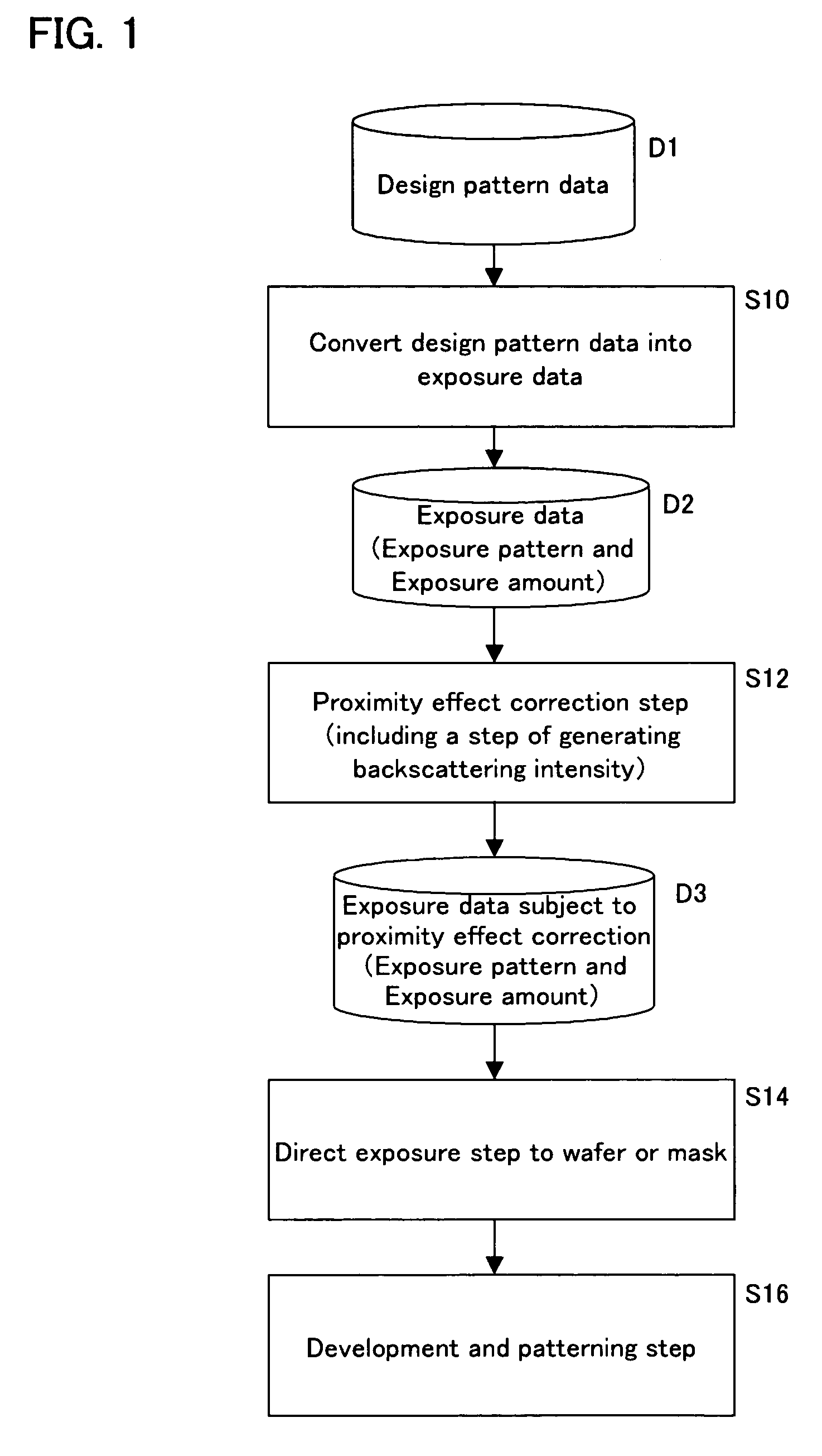
Method for generating backscattering intensity on the basis of lower layer structure in charged particle beam exposure, and method for fabricating semiconductor device utilizing this method
a charge particle and backscattering intensity technology, applied in the field of semiconductor device fabrication, can solve the problems of inability to provide accurate backscattering intensity determination and all methods are limited to simplified methods, so as to achieve simplified computation steps and shorten computation time
- Summary
- Abstract
- Description
- Claims
- Application Information
AI Technical Summary
Benefits of technology
Problems solved by technology
Method used
Image

Examples
second embodiment
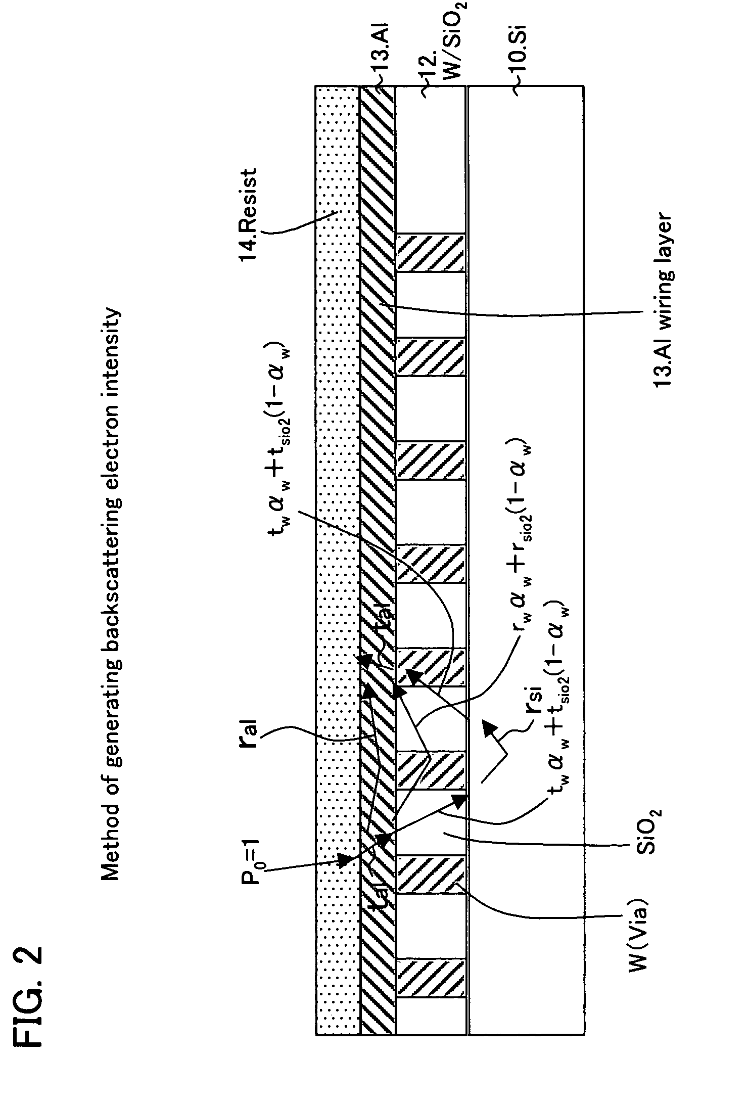
[0144][Second Embodiment]
[0145]According to the procedure for calculating the influence of backscattering in the first embodiment above, the electron number flow within the layers is calculated by defining the reflection coefficient, transmission coefficient, and scatter distribution of each constituent material in each layer and applying a weighting for the area density (occupancy) at which each material is present. That is, as shown in FIG. 10, the flow of the electron number P is combined layer by layer and calculated recursively from the uppermost layer to the lowermost layer. Further, the electron number P0′ that ultimately returns to the resist is the energy due to backscattering that is absorbed by the resist. According to this method, because the electron reflection, transmission and screening effects, and so forth, of each material of each layer are implemented, the backscattering intensity can be calculated accurately.
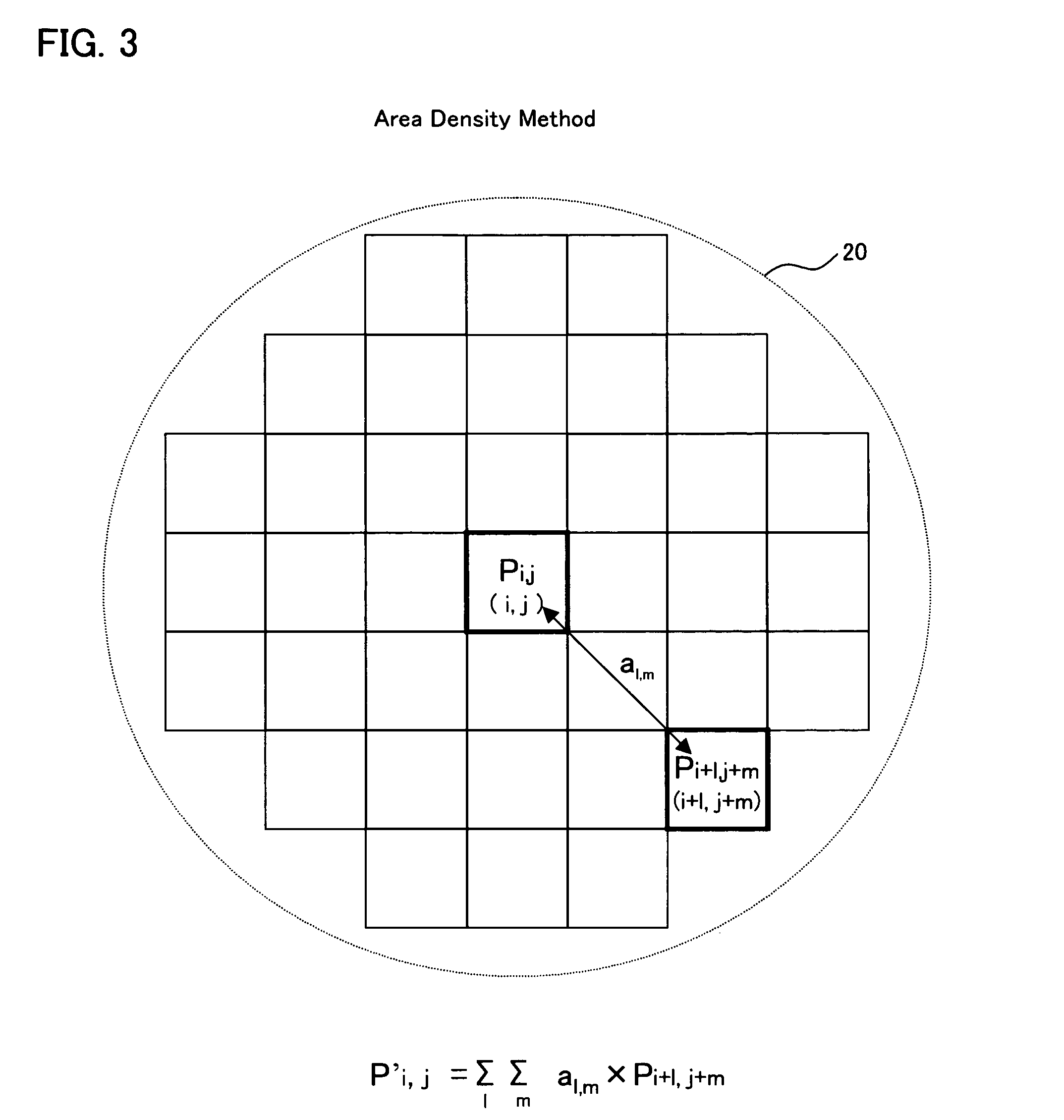
[0146]FIG. 16 illustrates the procedure for generating ...
PUM
| Property | Measurement | Unit |
|---|---|---|
| width | aaaaa | aaaaa |
| width | aaaaa | aaaaa |
| thickness | aaaaa | aaaaa |
Abstract
Description
Claims
Application Information