Electronic component and method of producing the same

a technology of electronic components and components, applied in the field of electronic components, can solve the problems of increasing the size of the package, increasing the size of the electronic component, and unable to provide wiring in the joining portions

Active Publication Date: 2007-04-17
MURATA MFG CO LTD
View PDF14 Cites 9 Cited by
  • Summary
  • Abstract
  • Description
  • Claims
  • Application Information

AI Technical Summary

Benefits of technology

[0013]To overcome the problems described above, preferred embodiments of the present invention provide an electronic component which includes a substrate, at least one piezoelectric vibrating portion and a connecting portion provided on the substrate, and a structural piece made of a resin material having a flat plate shape and covering at least the piezoele...

Problems solved by technology

However, the above-described structure increases the size of the package.
However, this increases the size of the electronic component.
However, the above-described electronic component including the piezoelectric substrate sealed with a glass member has the following problems.
Therefore, a wiring can not be provided in the joining portions.
Thus, the size of electronic component cannot be sufficiently reduced.
Thus, the moving ions greatly reduce the reliability of electronic component.
These processes greatl...

Method used


Image

  • Electronic component and method of producing the same
  • Electronic component and method of producing the same
  • Electronic component and method of producing the same

Examples


Embodiment Construction

[0037]Hereinafter, preferred embodiments of the present invention will be described in detail with reference to the accompanying drawing.

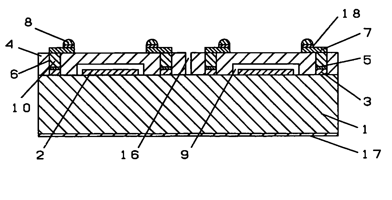
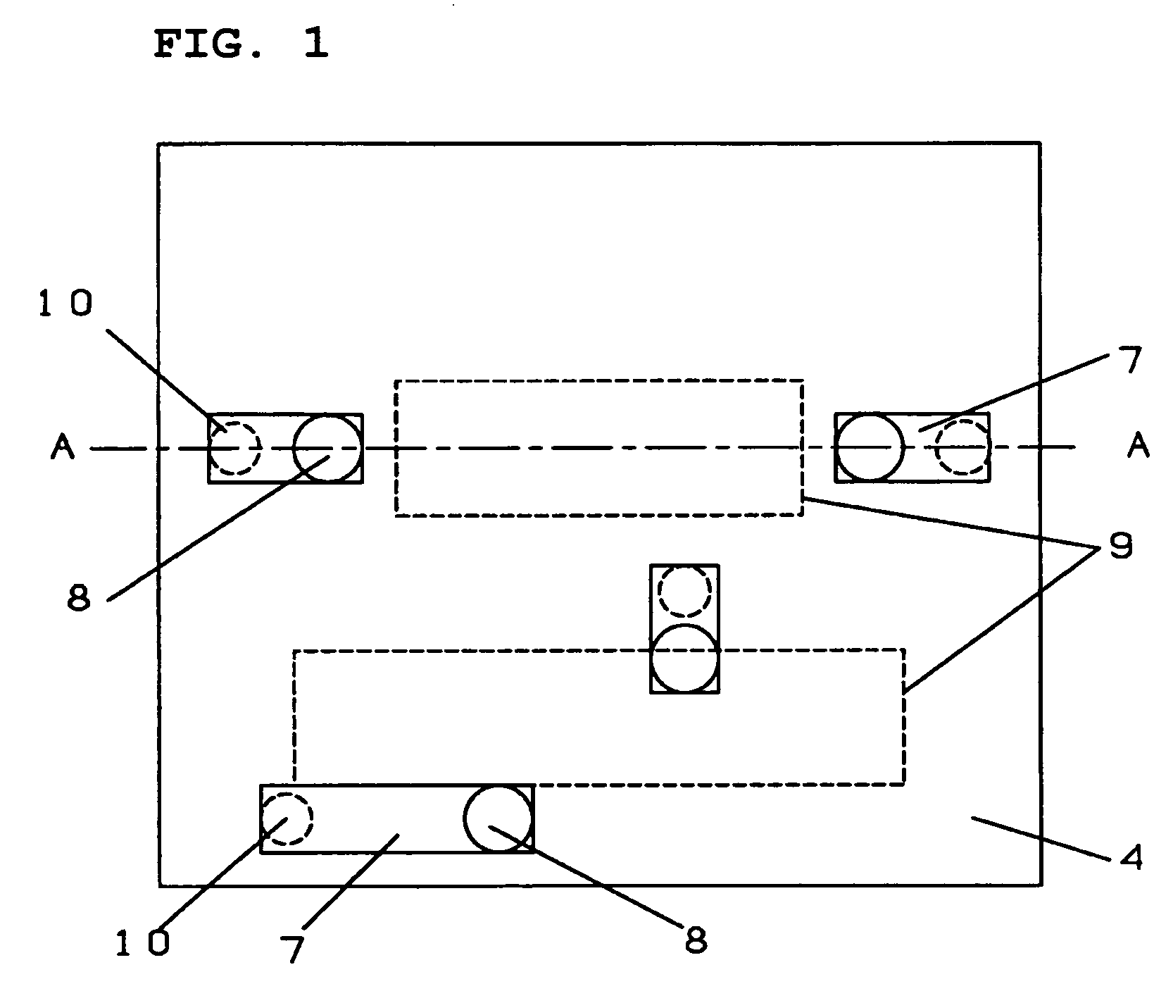
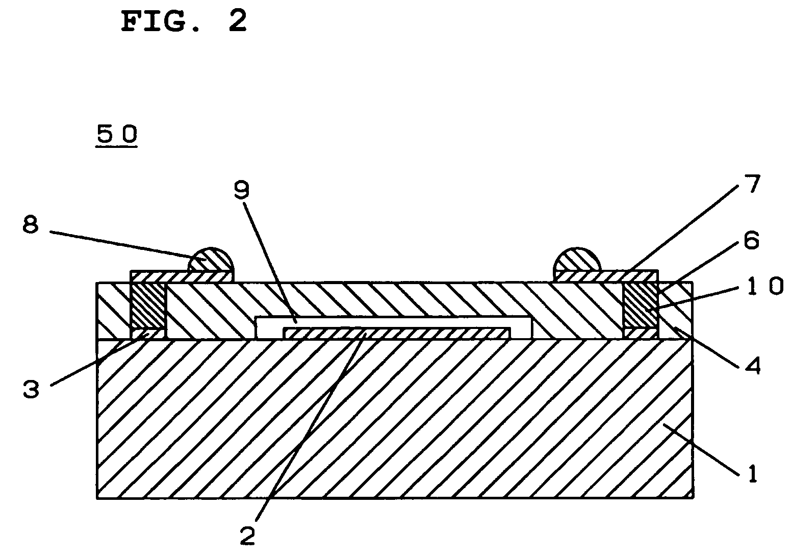
[0038]FIG. 1 is a schematic plan view of an electronic component according to a preferred embodiment of the present invention. FIG. 2 is a cross-sectional view taken along line A—A in FIG. 1.

[0039]Referring to FIGS. 1 and 2, an electronic component 50 includes a substrate 1 and a structural piece 4.

[0040]A plurality of IDT electrodes 2 and connecting portions 3 are provided on the substrate 1. The connecting portions 3 are electrically connected to the IDT electrodes 2. Thus, a desired function is performed. Moreover, electrodes having patterns and film-thicknesses suitable for desired functions are provided on the IDT electrodes 2. The patterns are not restricted to the IDT electrodes 2. The patterns may be applied to electrodes which define a piezoelectric vibrating portion.

[0041]Pads 5 are provided on the upper surfaces of the connecting portion...


PUM


Abstract

An electronic component includes at least one piezoelectric vibrating portion, a connecting portion provided on a substrate, a structural piece including a concavity so as not to disturb the vibration of the piezoelectric vibrating portion, and a connecting wiring for electrically connecting a pad on the substrate to a mounting wiring disposed on the upper surface of the structural piece. The structural piece further includes a through hole having an electroconductive material filled therein. The structural piece seals the piezoelectric vibrating portion.

Description

BACKGROUND OF THE INVENTION[0001]1. Field of the Invention[0002]The present invention relates to an electronic component for use in an electronic circuit in the communication field such as a portable telephone or a television, which includes at least one piezoelectric vibrating-portion and a connecting portion provided on a substrate.[0003]2. Description of the Related Art[0004]The basic structure of such electronic components includes a piezoelectric vibrating-portion provided on a substrate, which is accommodated in a package providing an air tight seal, in order to ensure its reliability.[0005]A portion of the package corresponding to the upper surface of the piezoelectric vibrating portion includes a space such that the vibration of the piezoelectric vibrating portion provided on the substrate is not disturbed. A package made of a metal or ceramic is used to ensure the reliability. However, the above-described structure increases the size of the package. This prevents size reduc...

Claims


Application Information

Patent Timeline
IPC IPC(8): H01L41/053H01L23/02H01L23/04H03H3/02H03H3/08H03H9/02H03H9/10H03H9/25
CPCH03H9/059H03H9/1092H01L2224/11H01L2224/05008H01L2224/05026H01L2224/0508H01L2224/05568H01L2224/05023H01L2224/05001H01L2224/05569H01L2224/05548H01L2224/05624H01L2924/00014H01L2224/05644H01L2224/05647H01L2224/05655H01L2224/05144H01L2224/05147H01L2224/05124H01L2924/01029H01L2924/013H01L2224/05111
Inventor IWAMOTO, TAKASHI
Owner MURATA MFG CO LTD
Why Eureka
Try Eureka