

Solid-state imaging apparatus and driving method thereof
- Summary
- Abstract
- Description
- Claims
- Application Information
AI Technical Summary
Benefits of technology
Problems solved by technology
Method used
Image

Examples
first embodiment
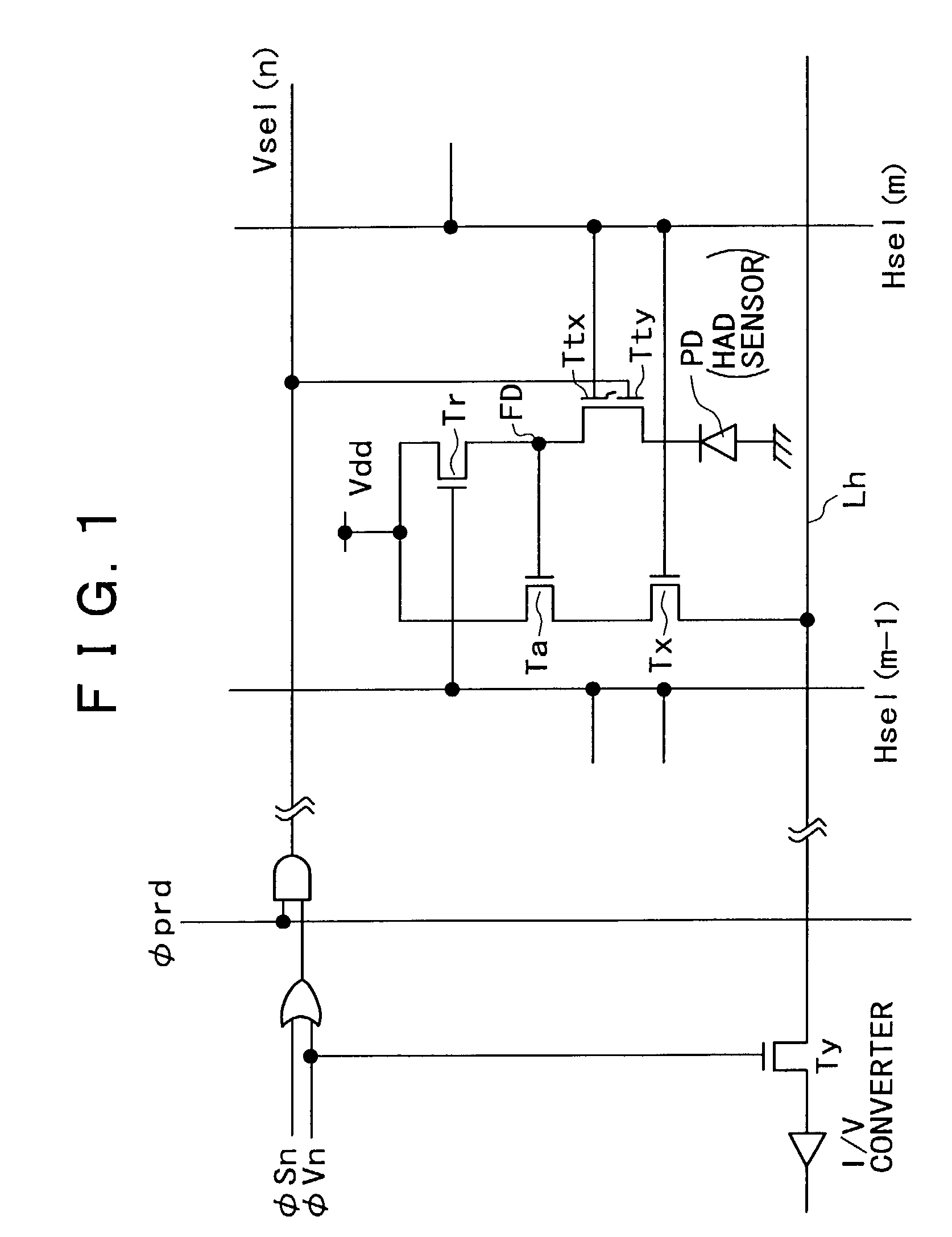
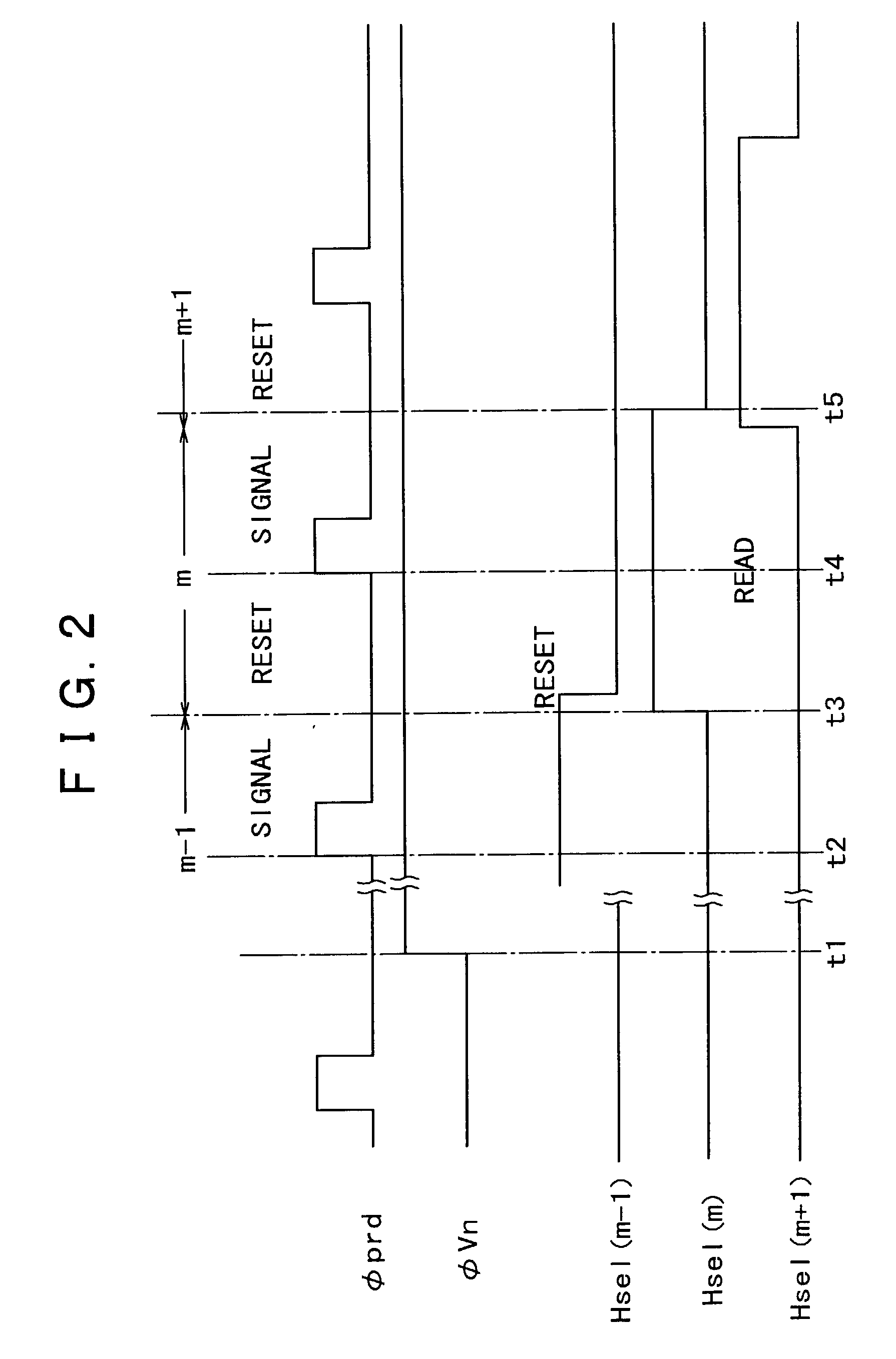
[0027]FIG. 1 is a circuit diagram showing a configuration of a unit pixel portion and its periphery in a MOS type solid-state imaging apparatus according to the present invention. FIG. 2 is a timing chart of operation timing of transistors within the unit pixel portion shown in FIG. 1.
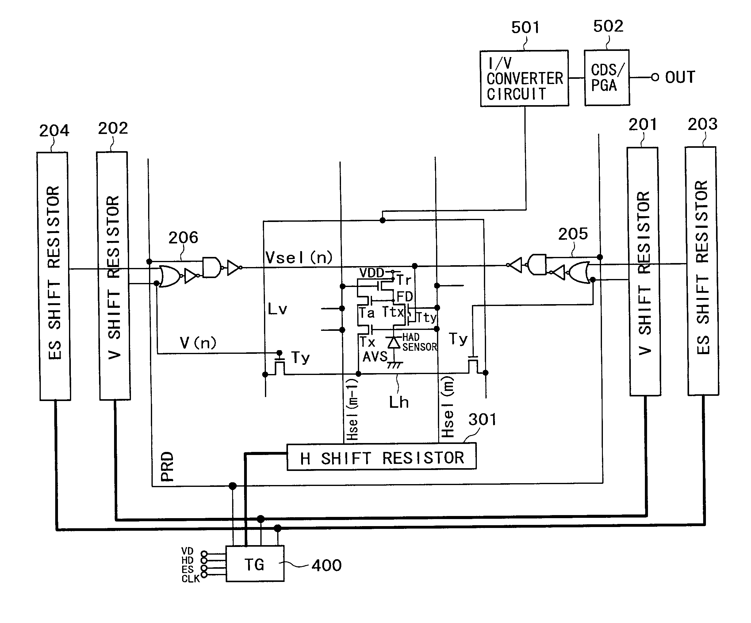
[0028]FIG. 3 is a block diagram schematically showing a configuration of the MOS type solid-state imaging apparatus provided with the unit pixel portion shown in FIG. 1.
[0029]A general configuration of the MOS type solid-state imaging apparatus according to the present embodiment will first be described with reference to FIG. 1 and FIG. 3.
[0030]The MOS type solid-state imaging apparatus in the first embodiment is formed with a large number of unit pixel portions (only one unit pixel portion is shown in the figures) arranged in a vertical direction and a horizontal direction in a matrix form, a V (vertical) scanner and an H (horizontal) scanner for reading a pixel signal from each of the unit pixel port...
second embodiment
[0064]the present invention will next be described.
[0065]The second embodiment is obtained by changing the signal wiring structure and contents of pulse signals of the first embodiment.
[0066]FIG. 5 is a circuit diagram showing a configuration of a unit pixel portion and its periphery in a MOS type solid-state imaging apparatus according to the second embodiment of the present invention. FIG. 6 is a timing chart of operation timing of transistors within the unit pixel portion shown in FIG. 5.
[0067]FIG. 7 is a block diagram schematically showing a configuration of the MOS type solid-state imaging apparatus provided with the unit pixel portion shown in FIG. 5.
[0068]Components common to FIGS. 5 to 7 and FIGS. 1 to 3 are identified by the same reference numerals.
[0069]In the solid-state imaging apparatus in the second embodiment, a reset / reading line RST / PRD for transmitting a reset pulse for driving a reset transistor Tr and a reading pulse for driving a reading selection transistor Ttx...
third embodiment
[0084]the present invention will next be described.
[0085]The third embodiment is obtained by changing the signal wiring structure and contents of pulse signals of the first embodiment.
[0086]FIG. 8 is a circuit diagram showing a configuration of a unit pixel portion and its periphery in a MOS type solid-state imaging apparatus according to the third embodiment of the present invention. FIG. 9 is a timing chart of operation timing of transistors within the unit pixel portion shown in FIG. 8.
[0087]FIG. 10 is a block diagram schematically showing a configuration of the MOS type solid-state imaging apparatus provided with the unit pixel portion shown in FIG. 8.
[0088]Components common to FIGS. 8 to 10 and FIGS. 1 to 3 are identified by the same reference numerals.
[0089]In the solid-state imaging apparatus in the third embodiment, a reading line PRD for transmitting a reading pulse for driving a reading selection transistor Ttx is arranged in correspondence with each column of unit pixels,...
PUM
 Abstract
Description
Claims
Application Information