MOS transistor apparatus and method of manufacturing same

Inactive Publication Date: 2005-03-22
HITACHI LTD
View PDF5 Cites 5 Cited by
  • Summary
  • Abstract
  • Description
  • Claims
  • Application Information

AI Technical Summary

Benefits of technology

If the semiconductor film is silicon germanium, then a polycrystalline silicon germanium film and a polysilicon film are formed after forming a silicon film in an island shape on the oxide film. It is particularly desirable that the silicon film has the form of fine grains of size 10 nm or less, or of amorphous particles. Thereby, it is possible to suppress depletion without the Ge atom concentration of the polycrystalline silicon germanium film declining by more than 20% from the film composition, in the vicinity of the interface with the oxide film. Moreover, the Ge atom concentration at the oxide film interface can be set to a uniform value of 80% or above in the monocrystalline particles, and the lattice distortion of the polycrystalline structure can be reduced and the stress reduced. If using an amorphous island-shaped silicon film, this can be achieved by per

Problems solved by technology

However, according to our research, it was found that at a polysilicon film forming temperature of 400-800° C., the initial nuclei of diameter 10 nm or less do not crystallize enough, and therefore, even if the concentration of nucleus generation is increased, particle growth will occur due to mutual bonding during film growth, and the resulting grain size in the vicinity of the oxide film interface after crystallization will not reduce below 30 nm.
If the film forming temperature is raised to 800° C. or above, then crystallization occurs, but such a temperature cannot be used, because the SiH4 starter material will decompose in the gas phase.
In particular, with silicon germanium films, the nucleus generation density is low on the oxide film, and hence the grains become coarser and it is difficult to reduce the grain size at the interface.
Introducing a silicon film is an effective method of preventing enlargement of the grains, but still the grain size cannot be reduced below 30 nm,

Method used


Image

  • MOS transistor apparatus and method of manufacturing same
  • MOS transistor apparatus and method of manufacturing same
  • MOS transistor apparatus and method of manufacturing same

Examples


Example

Second Embodiment

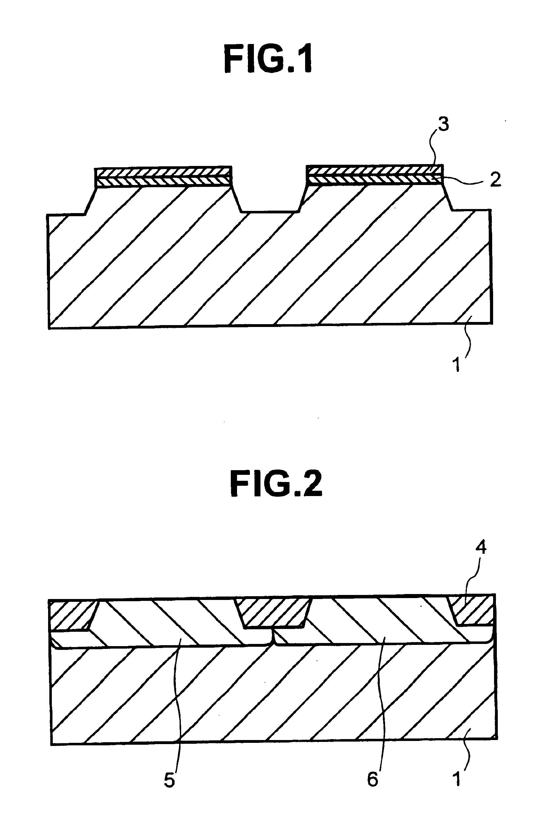
There follows a description of a method of manufacturing a CMOSFET using a fine polysilicon germanium film by supplying crystalline silicon fine particles according to the present invention. The methods for forming element separating grooves and wells are the same as those in the first embodiment, and hence they are omitted here and a detailed description of the polysilicon germanium film formation process is given.

In order to describe the benefits of the present invention, a comparison is made with the sequence for polysilicon germanium film formation based on supply of silicon fine particles according the first embodiment.

Example

FIG. 29 shows a gas flow for CVD film formation according to the first embodiment. After heating a wafer to a film formation temperature of 500-800° C., the temperature is held at a uniform value for approximately 10 seconds, and then SiH4 gas is introduced into the film formation chamber. When a silicon film of approximately 3-10 nm has been formed, GeH4 gas is introduced in such a manner that the Ge composition in the polysilicon germanium film will be 10-30%. A polysilicon germanium film is formed to a thickness of approximately 100-150 nm. The process of forming the polysilicon germanium film by supplying silicon fine particles is illustrated in FIG. 30. FIG. 30(a) illustrates a state after formation of silicon fine particles; FIG. 30(b) illustrates a state during forming of the polysilicon germanium film; and FIG. 30(c) illustrates a state after formation of the polysilicon germanium film. Under these film formation conditions, normally, a crystalline film is created, but since...

Example

Third Embodiment

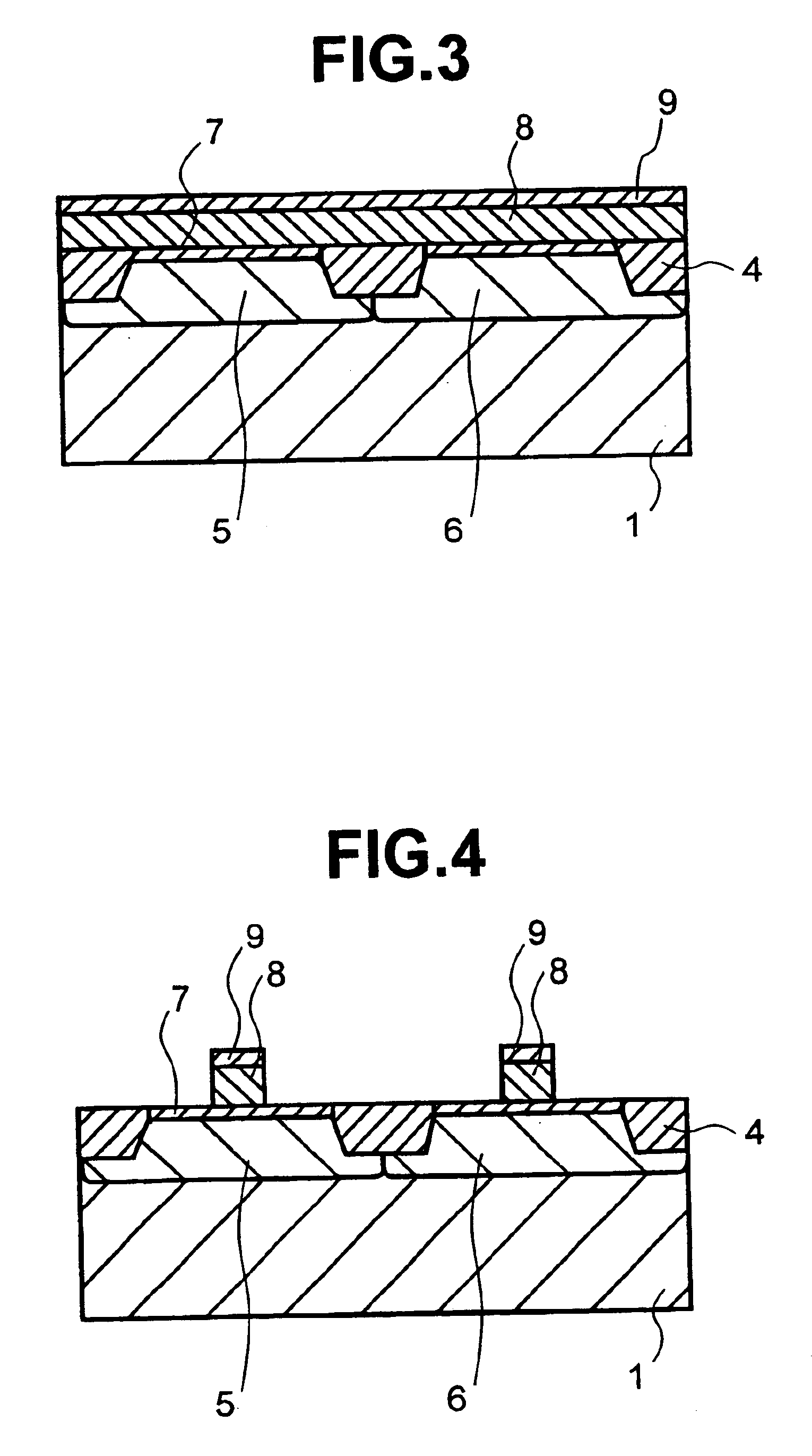
There follows a description of a method of manufacturing a CMOSFET using metal gate electrodes, which represents an embodiment of the present invention. The methods of forming the wells and element separating grooves are similar to those of the first embodiment, and hence they are omitted here and a detailed description of the formation of the metal gate electrodes is given.

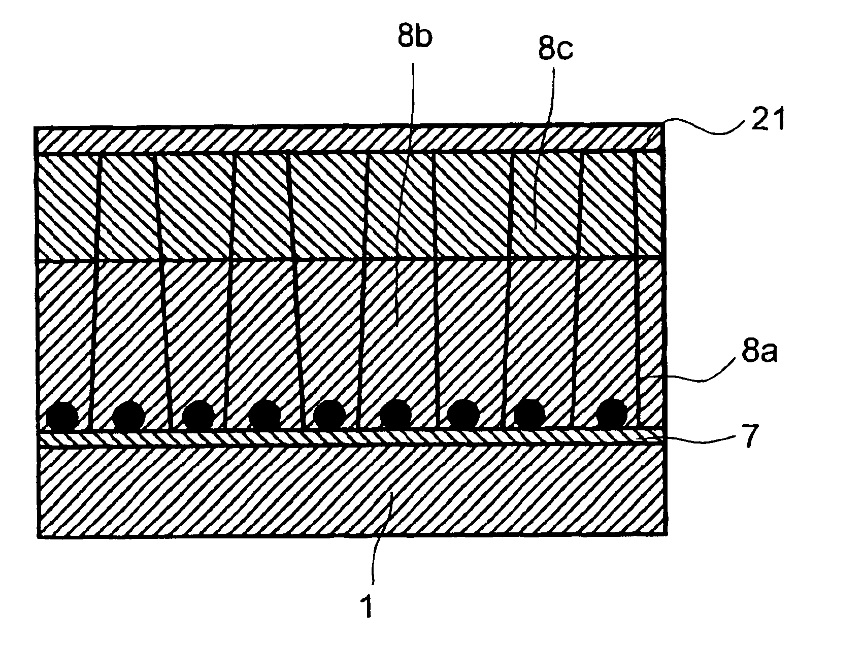
As shown in FIG. 40, a gate insulating film 7 comprising tantalum oxide is formed to approximately 5 nm by CVD on the surface of a p-type well 5 and an n-type well 6, and a gate electrode film 8 comprising tungsten is formed to approximately 50-100 nm by CVD. As shown in FIG. 41, a silicon nitride film 9 is deposited on the gate electrode film 8, and the silicon nitride film 9 and gate electrode film 8 are dry etched using a resist mask to form gate electrodes.

FIG. 42 shows a gas flow for tungsten film formation according to the third embodiment. The supply of WCl4 gas is hearted for a period, and...


PUM


Abstract

When polycrystalline silicon germanium film is used for gate electrodes in a MOS transistor apparatus, there have been problems of reduced reliability in the gate insulating film, due to stress in the silicon germanium grains. Therefore, a polysilicon germanium film is formed, after forming silicon fine particles of particle size 10 nm or less on an oxide film. As a result, it is possible to achieve a high-speed MOS transistor apparatus using an ultra-thin oxide film having a film thickness of 1.5 nm or less, wherein the Ge concentration of the polycrystalline silicon germanium at its interface with the oxide film is uniform, thereby reducing the stress in the film, and improving the reliability of the gate electrode.

Description

BACKGROUND OF THE INVENTION1. Field of the InventionThe present invention relates to a highly reliable MOS transistor devices wherein a semiconductor film and metallic film comprising fine crystals are used as a gate electrode.2. Description of the Related ArtGate oxide films in MOSFETs (Metal Oxide Semiconductor Field Emission Transistor, hereinafter, abbreviated as “MOS transistor”) have successively been reduced in thickness on the basis of the scaling rule proposed by R. Dennard, but at thicknesses of 3 nm or less, there have been concerns regarding the increase in leakage current due to tunnel effects at low voltages. However, it has been confirmed that even if a tunnel current is flowing, a MOS transistor devices can be made to operate normally by shortening the gate length, and MOS transistor devices using gate oxide films of 1.5 nm or less have been achieved. Investigation has also been conducted into oxide equivalents of 1.0 nm or less, wherein materials such as silicon nit...

Claims


Application Information

Patent Timeline
IPC IPC(8): H01L21/70H01L21/02H01L21/28H01L21/8238H01L21/285H01L27/092H01L29/423H01L29/49H01L29/78
CPCH01L21/2807H01L21/823857H01L21/823828
Inventor KANDA, NAOKIOGAWA, ARITONISHITANI, EISUKENAKAHARA, MIWAKOYOSHIDA, TADANORIOGATA, KIYOSHI
Owner HITACHI LTD
Why Eureka
Try Eureka