Nickel silicide including indium and a method of manufacture therefor

a technology of nickel silicide and indium, which is applied in the direction of semiconductor devices, bulk negative resistance effect devices, electrical appliances, etc., can solve the problems of nickel silicide excessive spike defects, high diffusivity of nickel silicide, and high defect density of nickel silicide, so as to reduce the number of defects

Active Publication Date: 2007-05-01
TEXAS INSTR INC
View PDF4 Cites 35 Cited by
  • Summary
  • Abstract
  • Description
  • Claims
  • Application Information

AI Technical Summary

Problems solved by technology

Nickel, unfortunately, has a very high diffusivity in silicon leading to the formation of nickel silicide regions that extend beneath the transistor sidewall structures.
Regrettably, the nickel silicide regions that extend beneath the transistor sidewall structures tend to lead to nickel silicide excessive encroachment defects extending into the channel region of the MOS transistor.
In a similar manner, the high diffusivity of nickel causes excessive spike defects into the source / drain regions.
As would be expected, the encroachment and spike defects tend to cause serious acceptance, manufacturability, and ultimately device yield problems.

Method used


Image

  • Nickel silicide including indium and a method of manufacture therefor
  • Nickel silicide including indium and a method of manufacture therefor
  • Nickel silicide including indium and a method of manufacture therefor

Examples


Embodiment Construction

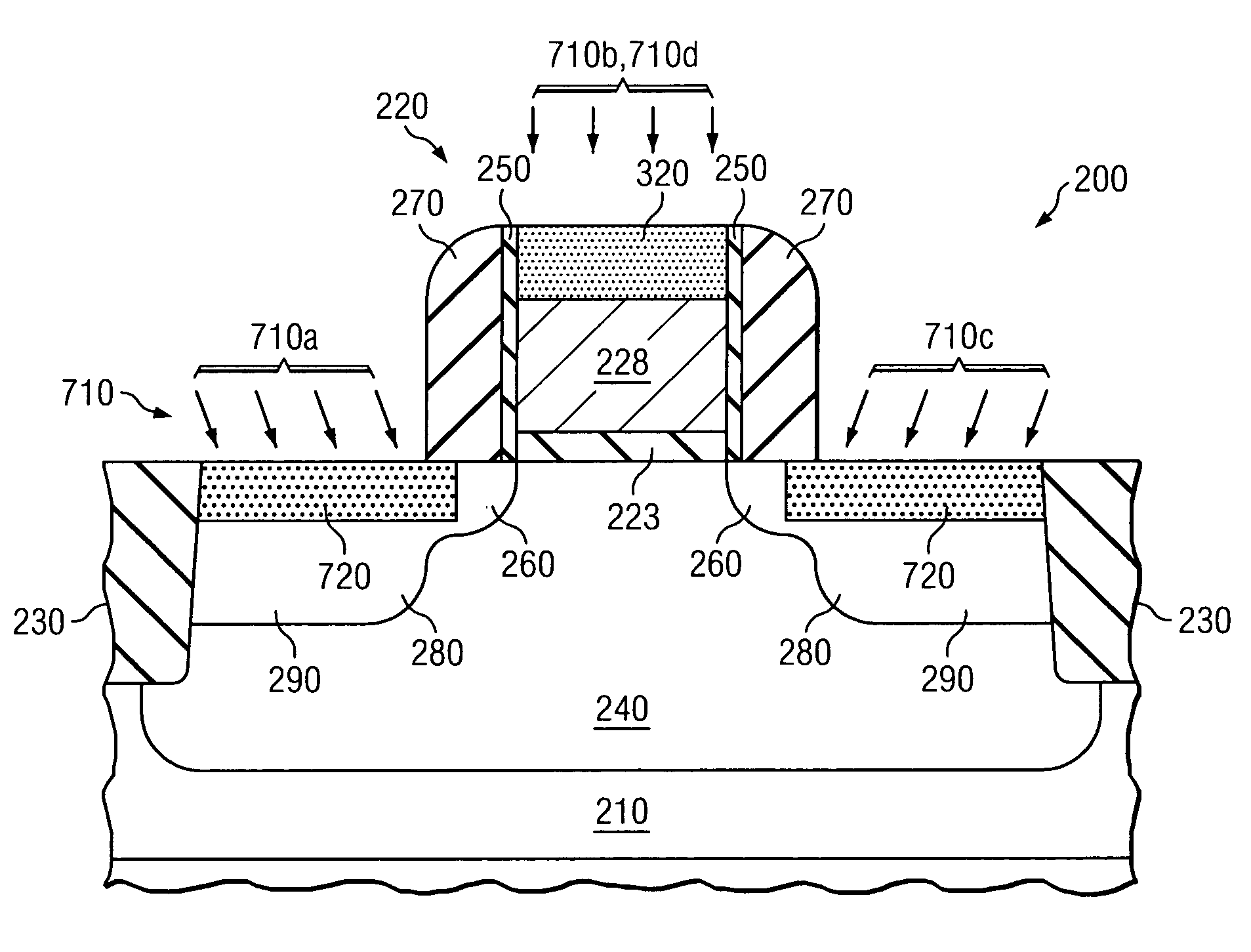
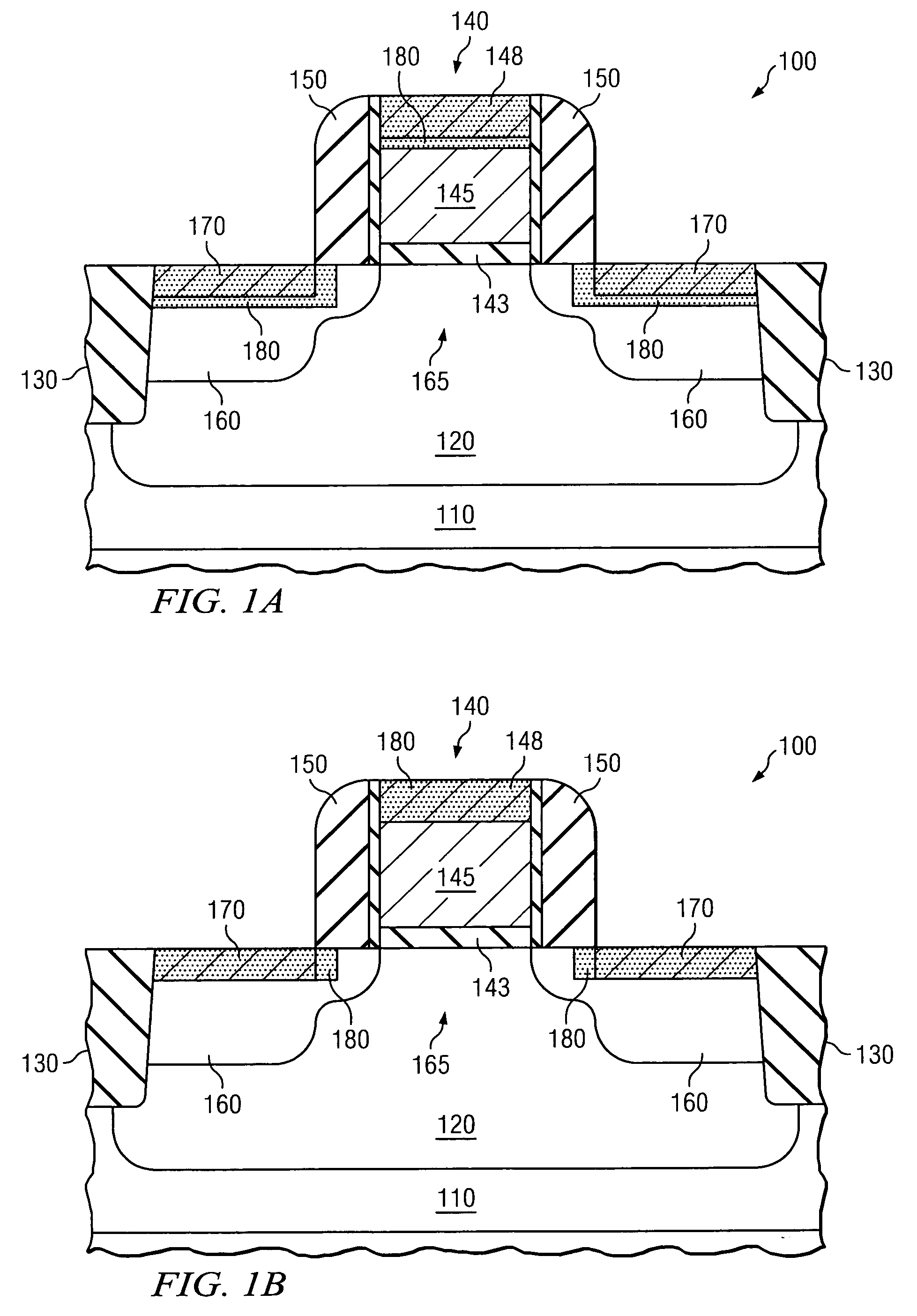
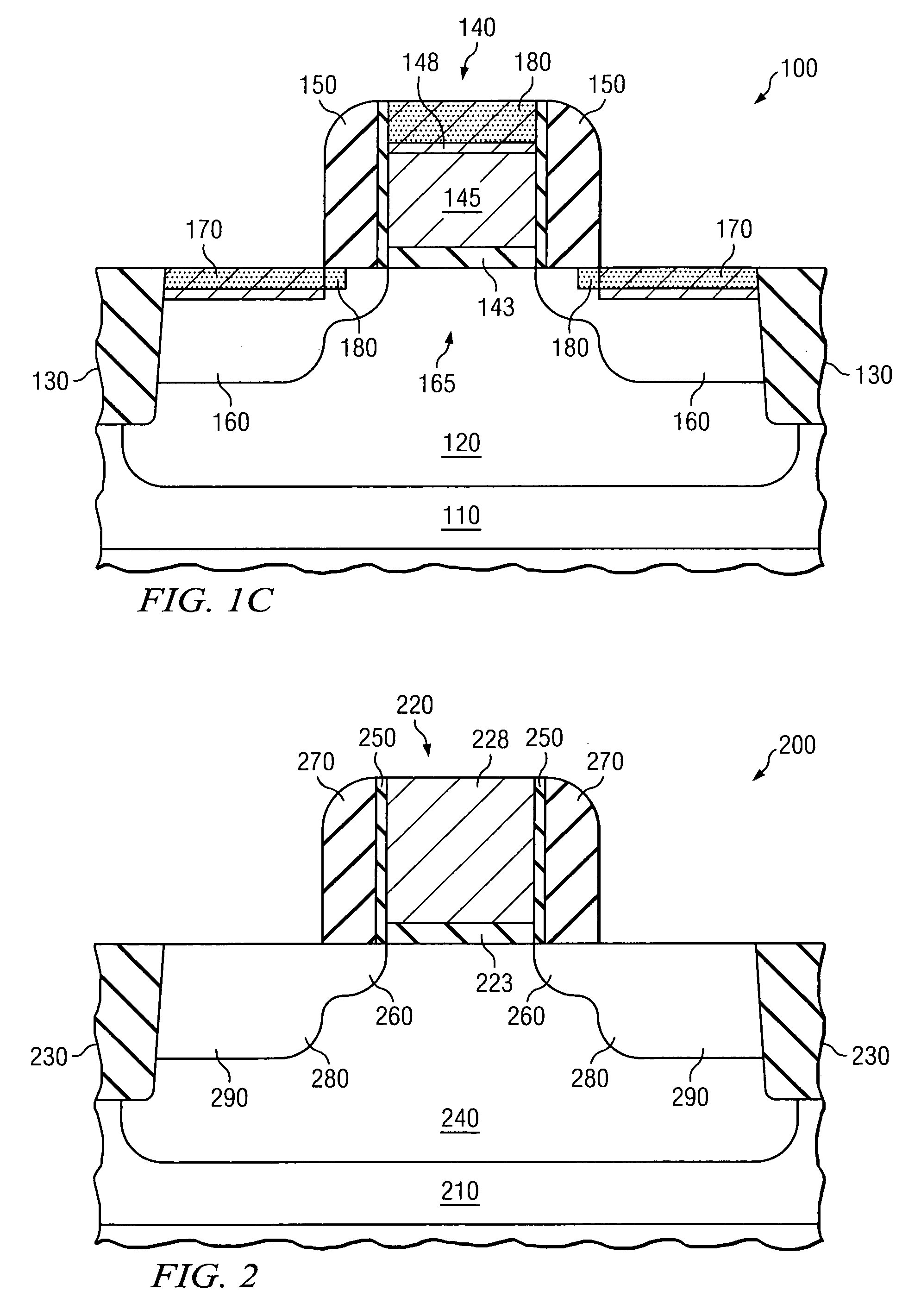
[0016]The present invention is based, at least in part, on the inclusion of indium into a nickel silicided formation process. The inclusion of indium into a region about to be silicided with nickel, substantially retards encroachment defects, or sometimes called piping defects, as well as spike defects that have only recently been attributed to the high diffusivity of nickel. Accordingly, indium, as compared to certain other dopants including antimony and germanium, provides unexpected results in that it not only causes the silicided region to form uniformly as both antimony and germanium do, but it additionally retards the undesirable encroachment and spike defects. Moreover, indium unexpectedly provides a lower resistance contact between the silicided region and the source / drain region or the gate electrode layer, than that previously obtained by any other method. Thus, the use of indium does not introduce the contact resistance degradation that may occur with antimony, germanium ...


PUM

PropertyMeasurementUnit
energyaaaaaaaaaa
implant angleaaaaaaaaaa
temperatureaaaaaaaaaa

Abstract

The present invention provides a semiconductor device, a method of manufacture therefore and a method for manufacturing an integrated circuit including the same. The semiconductor device, among other elements, may include a substrate (110), as well as a nickel silicide region (170) located over the substrate (110), the nickel silicide region (170) having an amount of indium located therein.

Description

TECHNICAL FIELD OF THE INVENTION[0001]The present invention is directed, in general, to a method for manufacturing a semiconductor device and, more specifically, to an improved nickel silicided including indium, a method of manufacture therefore, and a method for manufacturing an integrated circuit including the same.BACKGROUND OF THE INVENTION[0002]Traditional metal-oxide-semiconductor (MOS) transistors often use metal silicide layers to reduce resistance. A self-aligned silicidation process (salicide) is often used to form the region of titanium, cobalt or tungsten silicide on the gate electrode and source / drain regions of the MOS transistor. In this process, a blanket metal film is deposited on the silicon substrate containing the MOS transistor structure. The metal is then reacted with the underlying silicon regions to form a low resistance metal silicide. Any unreacted metal remaining on the substrate is then removed using a metal etch process that is selective to the remaining...

Claims


Application Information

Patent Timeline
Patent Type & Authority Patents(United States)
IPC IPC(8): H01L21/44
CPCH01L21/26586H01L21/28518H01L29/665H01L29/6656H01L29/6659H01L29/7833
Inventor CHEN, PEIJUN J.YUE, DUOFENGJAIN, AMITABHCRANK, SUEBONIFIELD, THOMAS D.MOGUL, HOMI
Owner TEXAS INSTR INC
Why Eureka
Try Eureka