

Method for manufacturing semiconductor device
a manufacturing method and semiconductor technology, applied in semiconductor/solid-state device manufacturing, basic electric elements, electric devices, etc., to achieve the effect of improving the patterning of the film to be processed and high yield
- Summary
- Abstract
- Description
- Claims
- Application Information
AI Technical Summary
Benefits of technology
Problems solved by technology
Method used
Image

Examples
first embodiment
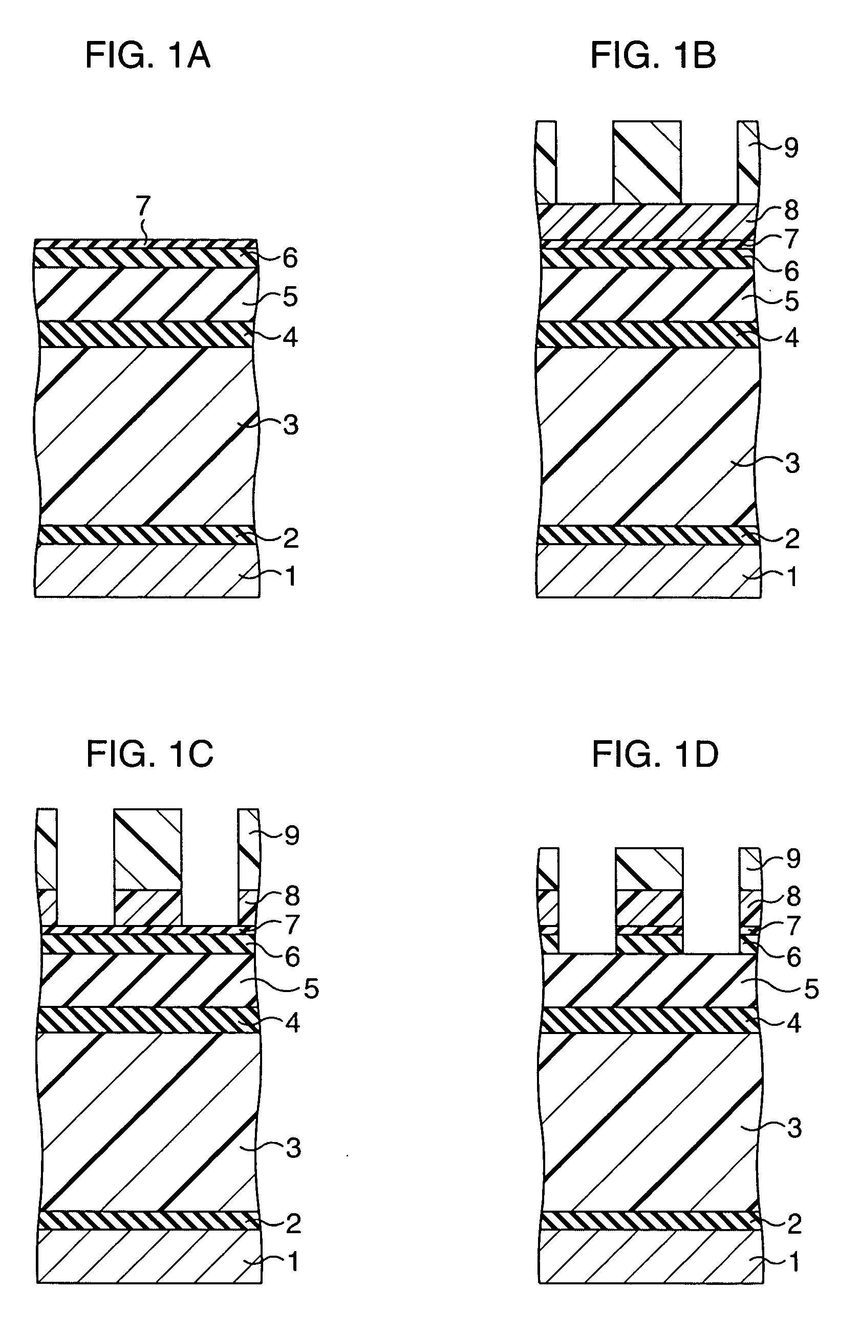
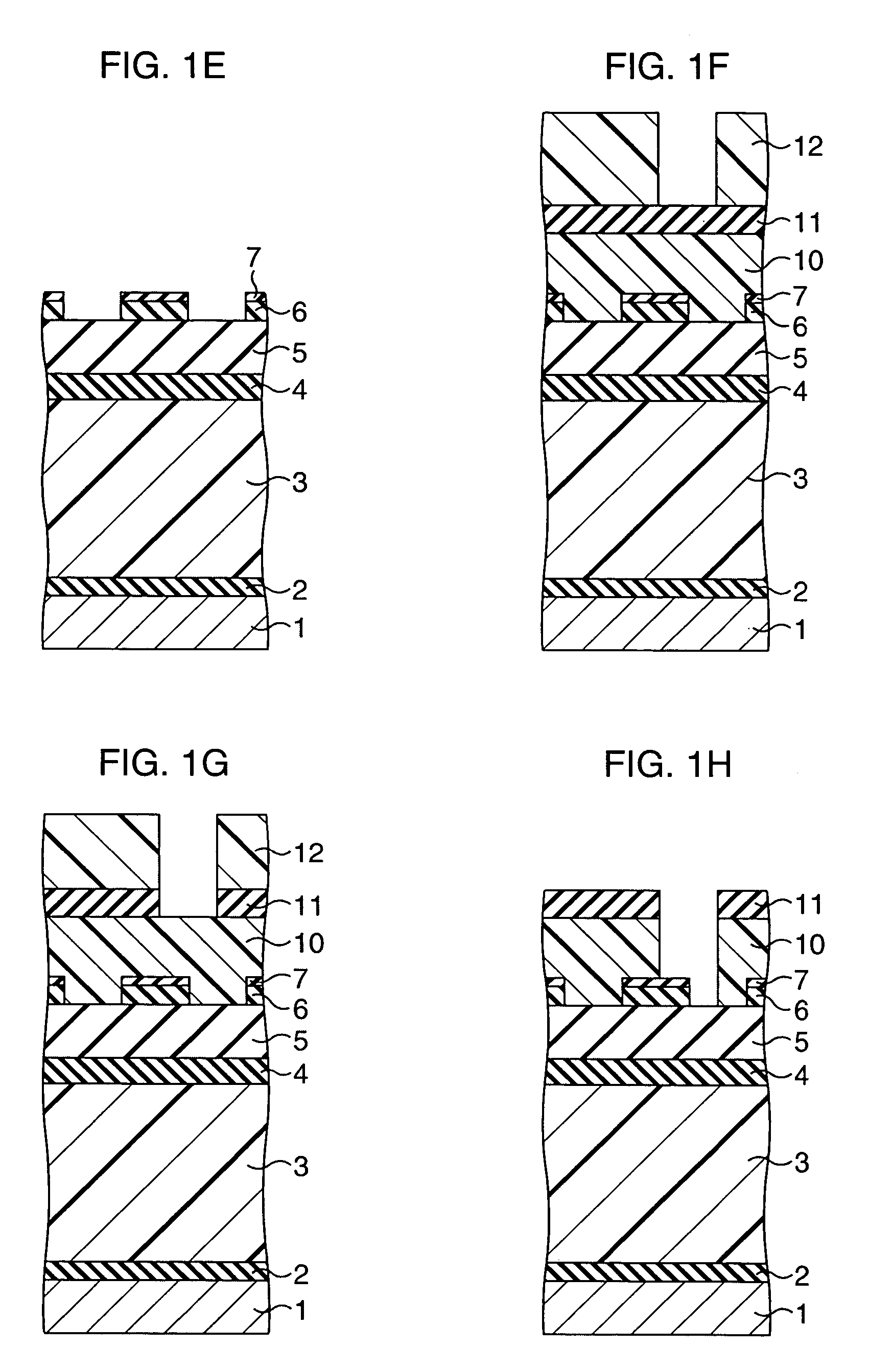
[0024](First Embodiment)
[0025]First, a first embodiment of the present invention is explained. FIG. 1A to FIG. 1Q are sectional views sequentially showing process steps of a method for manufacturing a semiconductor device according to a first embodiment of the present invention. In the embodiment, a semiconductor device is manufactured by a trench-first hard mask dual damascene method. Here, in the trench-first hard mask method, a hard mask pattern for forming a wiring trench pattern is formed on an interlayer insulating film in advance, then a via is patterned directly on a level difference of the wiring trench pattern, and then a via is processed and a trench is processed in the interlayer insulating film in this order, thereby a dual damascene structure is formed.
[0026]As shown in FIG. 1A, an SiC film 2 as an etching stopper film is first formed on a Cu wiring 1. The SiC film 2 is, for example, 30 nm thick. Then, an organic low dielectric constant film 3 is formed on the SiC film...
second embodiment
[0052](Second Embodiment)
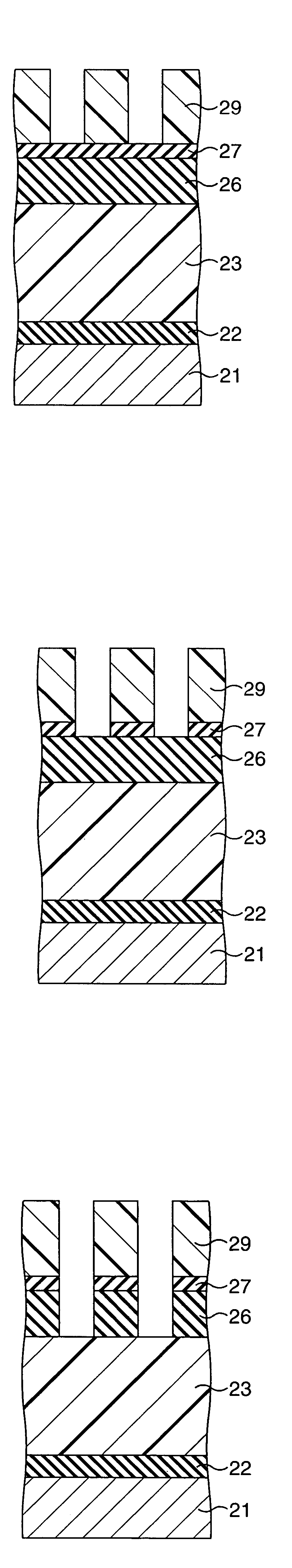
[0053]Next, the second embodiment of the present invention will be described. FIG. 3A to FIG. 3K are sectional views sequentially showing process steps of a method for manufacturing a semiconductor device according to a second embodiment of the present invention. In this embodiment, a semiconductor device is manufactured by a single damascene method.
[0054]As shown in FIG. 3A, a SiC film 22 is first formed as an etching stopper film on a Cu wiring 21.
[0055]Next, an organic low dielectric constant film 23 is formed as an interlayer insulating film (a film to be processed) on the SiC film 22. Subsequently, a silicon nitride film 26 is formed as a hard mask (a first mask film) on the organic low dielectric constant film 23, for example, by a plasma CVD method.
[0056]Thereafter, as shown in FIG. 3B, a silicon oxide film (an oxide layer) 27 is formed on the surface of the silicon nitride film 26 by performing O2 plasma processing to a surface of the silicon nitride...
PUM
| Property | Measurement | Unit |
|---|---|---|
| dielectric constant | aaaaa | aaaaa |
| thick | aaaaa | aaaaa |
| thick | aaaaa | aaaaa |
Abstract
Description
Claims
Application Information