Method and apparatus for mode conversion

a mode conversion and mode technology, applied in the field of mode conversion, can solve the problems of time-consuming and expensive process, complex fabrication of vertical taper in semiconductors, and high cost of optical components and their precise assembly, and achieve the effect of high transmissivity

Active Publication Date: 2007-05-08
WSOU INVESTMENTS LLC +1
View PDF13 Cites 11 Cited by
  • Summary
  • Abstract
  • Description
  • Claims
  • Application Information

AI Technical Summary

Benefits of technology

[0012]To provide some spot placement adjustment, each waveguide between the two star couplers can be provided with a controllable phase shifter. Movement of the spot laterally is accomplished by applying a linear phase shift distribution across the connecting waveguides, and spot focus is adjusted by applying a parabolic phase shift distribution across the connecting waveguides. If the connecting waveguides have a substantial path-length difference between adjacent waveguides, so as to provide a grating function, one can further provide wavelength tunability, by adjusting the phase shifters. A linear phase shift distribution moves the wavelength comb of the grating, and, if the grating is chirped, a parabolic phase shift distribution can change which grating order has the highest transmissivity.

Problems solved by technology

The use of lenses to mode convert has several drawbacks, including the expense of the optical components and their precise assembly and the need to hermetically package the interface.
However, fabricating a vertical taper in a semiconductor is a complex, time consuming and expensive process and often requires an SOA performance trade-off.
While these lasers have adequate performance, they require complex InP growth and processing, time-consuming testing and calibration, sensitive control, and an external wavelength monitor.
While such lasers are relatively inexpensive, the above-noted challenges make the price too high for applications such as fiber-to-the-home.
These lasers also have adequate performance, but require significant hand assembly and have moving parts.
The disadvantages of this approach include complicated processing, limited wavelength tuning, and low output power.

Method used


Image

  • Method and apparatus for mode conversion
  • Method and apparatus for mode conversion
  • Method and apparatus for mode conversion

Examples


Embodiment Construction

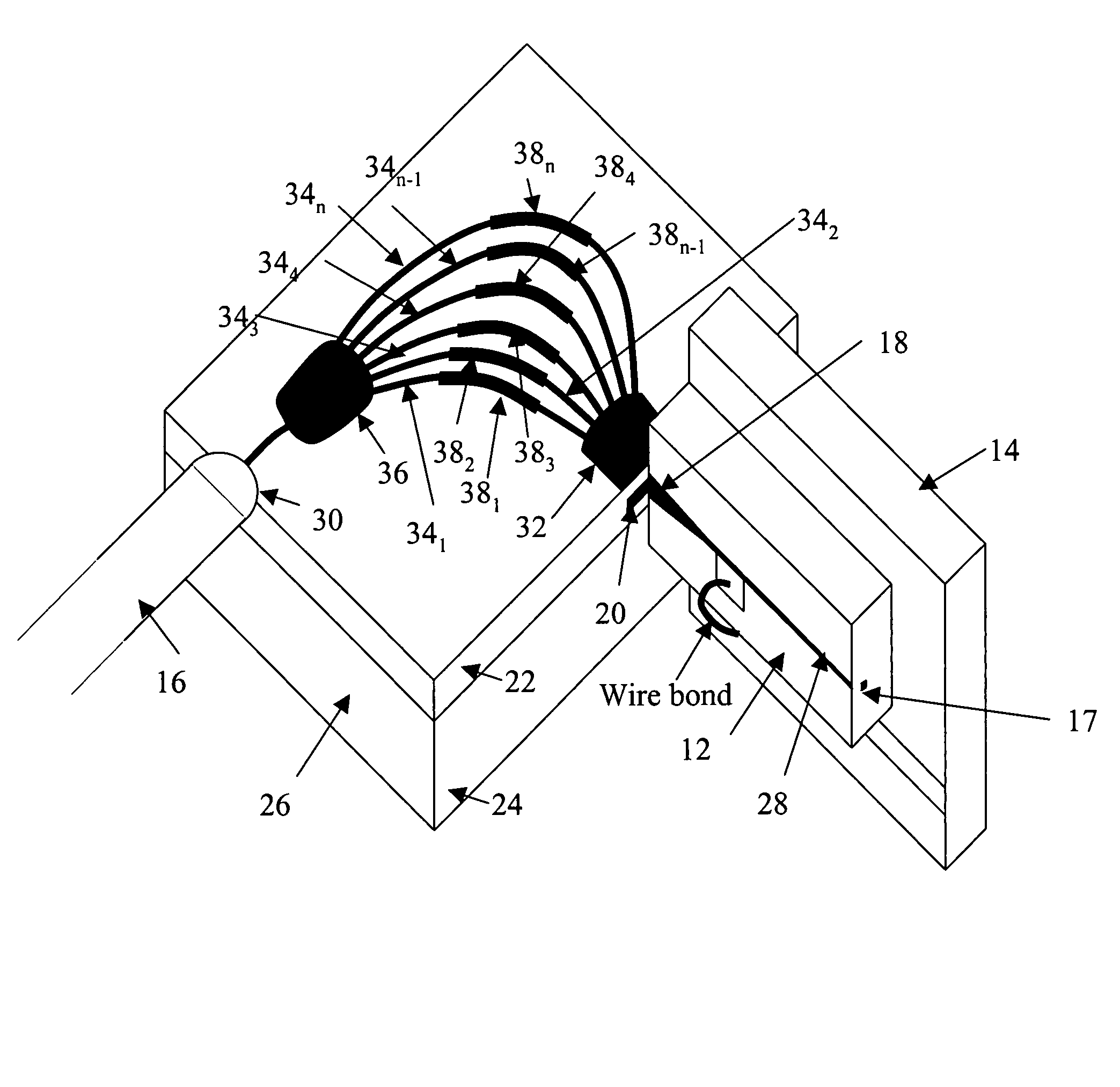
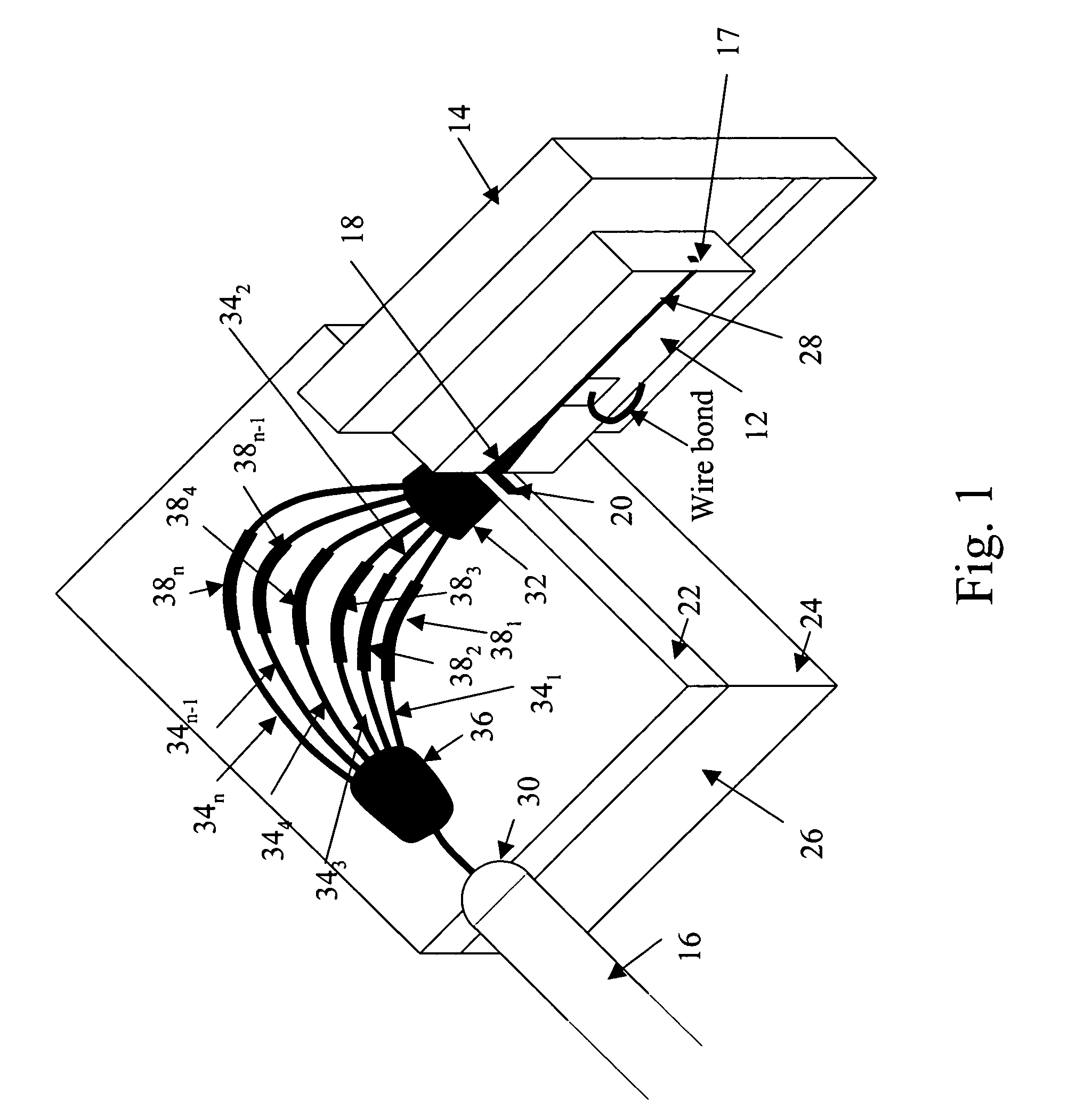
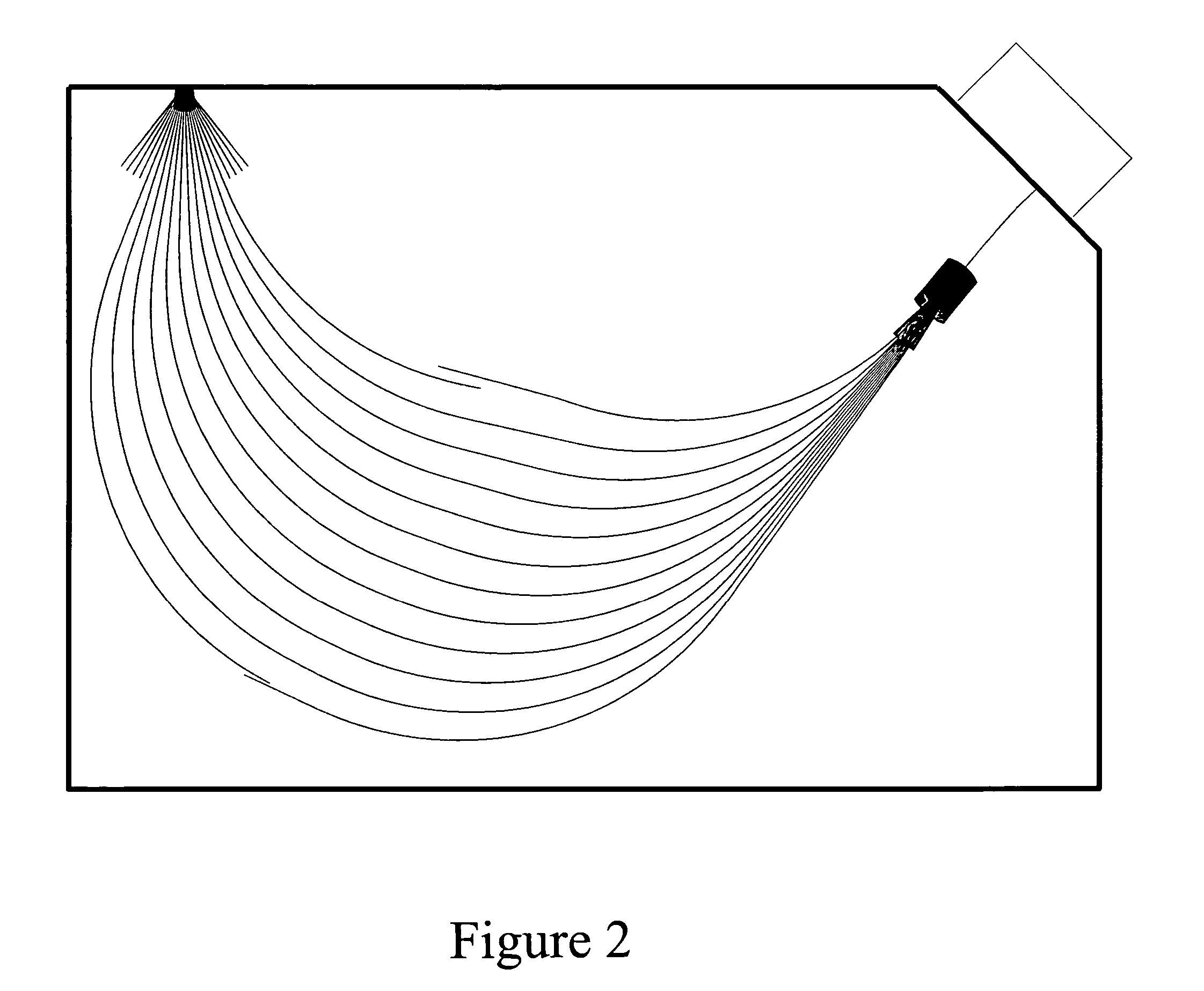
[0019]FIG. 1 illustrates the basic components of a wavelength tunable laser with mode conversion in accordance with a particular embodiment of the present invention. An optical element with a relatively high refractive index, such as a semiconductor optical device, and, more particularly, a semiconductor optical amplifier (SOA) 12 is mounted on a submount 14. The SOA may comprise any form, but in one preferred embodiment is formed in InP waveguides. In the illustrated embodiment, the light output from the SOA 12 is to be coupled to another optical element having a lower refractive index, such as an optical fiber 16. Accordingly, the mode or spot size of the beam in the SOA 12 is smaller than the mode or spot size in the fiber 16. The output media does not necessarily have to comprise an optical fiber, but can take many other forms, including waveguides, silica planar waveguides, another semiconductor, etc. The SOA 12 has an output facet 18 coupled to a facet 20 in a silica waveguide...


PUM


Abstract

Spot-size conversion for interfacing a first optical element having a higher refractive index to a second optical element having a lower refractive index is achieved through the use of two optical star couplers coupled to each other through a plurality of optical paths embedded in a planar waveguide. The beam from the high refractive index element is introduced into a high numerical aperture (NA) star coupler, which directs the beam through a plurality of optical paths to a second star coupler with a lower numerical aperture than the first star coupler so that its output spot-size is larger. The output port of the second star coupler is interfaced to the lower refractive index element. Wavelength selection can be provided by making non-zero path-length differences between adjacent optical paths between the two star couplers. Wavelength tunability can be provided by including phase shifters in the paths between the two star couplers to alter the effective optical lengths of the paths to selectively produce the desired phase interference pattern at the desired wavelength.

Description

RELATED APPLICATIONS[0001]This application is a continuation-in-part of U.S. patent application Ser. No. 10 / 641,519, filed Aug. 15, 2003.FIELD OF THE INVENTION[0002]The invention pertains to mode conversion between different waveguide devices. More particularly, the invention pertains to mode conversion and frequency tuning of semiconductor lasers.BACKGROUND OF THE INVENTION[0003]In optical networks and other environments, it often is necessary to interface semiconductor optical amplifiers and other semiconductor optical devices to optical fibers, silica planar optical waveguides, and other optical media. These various optical devices and media often have different propagation modes and thus require mode (or spot-size) conversion in order to interface to each other. For instance, optical seminconductor devices such as a semiconductor optical amplifier (SOA) typically have a very small spot size (or mode) compared to an optical fiber or a silica planar optical waveguide. One applicat...

Claims


Application Information

Patent Timeline
Patent Type & Authority Patents(United States)
IPC IPC(8): G02B6/26G02B6/42G02B6/30G02B6/34
CPCG02B6/12011G02B6/12019G02B6/12033G02B6/30G02B6/4201
Inventor DOERR, CHRISTOPHER RICHARDSTULZ, LAWRENCE WARREN
Owner WSOU INVESTMENTS LLC
Why Eureka
Try Eureka