Method for forming film, method for forming wiring pattern, method for manufacturing semiconductor device, electro-optical device, and electronic device

a technology of wiring pattern and forming method, which is applied in the field of forming film, can solve the problems of poor quality transferring and the entire transferring layer to be transferred, and achieve the effects of saving material consumption, efficient conversion into thermal energy, and relieving vacuum

Active Publication Date: 2007-05-15
INTELLECTUAL KEYSTONE TECH LLC
View PDF18 Cites 42 Cited by
  • Summary
  • Abstract
  • Description
  • Claims
  • Application Information

AI Technical Summary

Benefits of technology

[0007]To address or resolve the above discussed and / or other problems, a method to form a film according to exemplary embodiments of the present invention, in which a transferring layer formed on a substrate is transferred to a workpiece to form a predetermined film on the workpiece, includes treating a surface of the workpiece to enhance or improve the adhesion between the transferring layer and the workpiece by chemical interaction. According to exemplary embodiments of the present invention, the transferring layer is transferred to the workpiece to form a film including the transferring layer. In particular, the surface treatment of the workpiece to enhance or improve the adhesion between the workpiece and the transferring layer by chemical interaction allows for high-quality transferring, preventing or inhibiting defective conditions, such as detachment of the transferred film from the surface of the workpiece.
[0024]An electro-optical device of exemplary embodiments of the present invention has the wiring pattern formed by the method to form a wiring pattern. Furthermore, the electro-optical device of exemplary embodiments of the present invention has the semiconductor device that is manufactured by the method to manufacture a semiconductor device. In addition, an electronic device of exemplary embodiments of the present invention has the electro-optical device. Exemplary embodiments of the present invention provide an electro-optical device that is efficiently manufactured and is highly reliable, and the electronic device that includes the electro-optical device. Exemplary examples of the electro-optical device include liquid crystal displays, organic electroluminescent (EL) displays, and plasma displays.

Problems solved by technology

Decreased adhesive strength between a substrate and a transferring layer may cause the entire transferring layer to be transferred to the workpiece without patterning.
Decreased adhesive strength between a transferring layer and a workpiece may result in poor-quality transferring and at the worst in a defective condition in which no transferring occurs.

Method used


Image

  • Method for forming film, method for forming wiring pattern, method for manufacturing semiconductor device, electro-optical device, and electronic device
  • Method for forming film, method for forming wiring pattern, method for manufacturing semiconductor device, electro-optical device, and electronic device
  • Method for forming film, method for forming wiring pattern, method for manufacturing semiconductor device, electro-optical device, and electronic device

Examples


Embodiment Construction

Method to Form a Film

[0038]The method to form a film according to exemplary embodiments of the present invention will now be further illustrated with reference to the attached drawings.

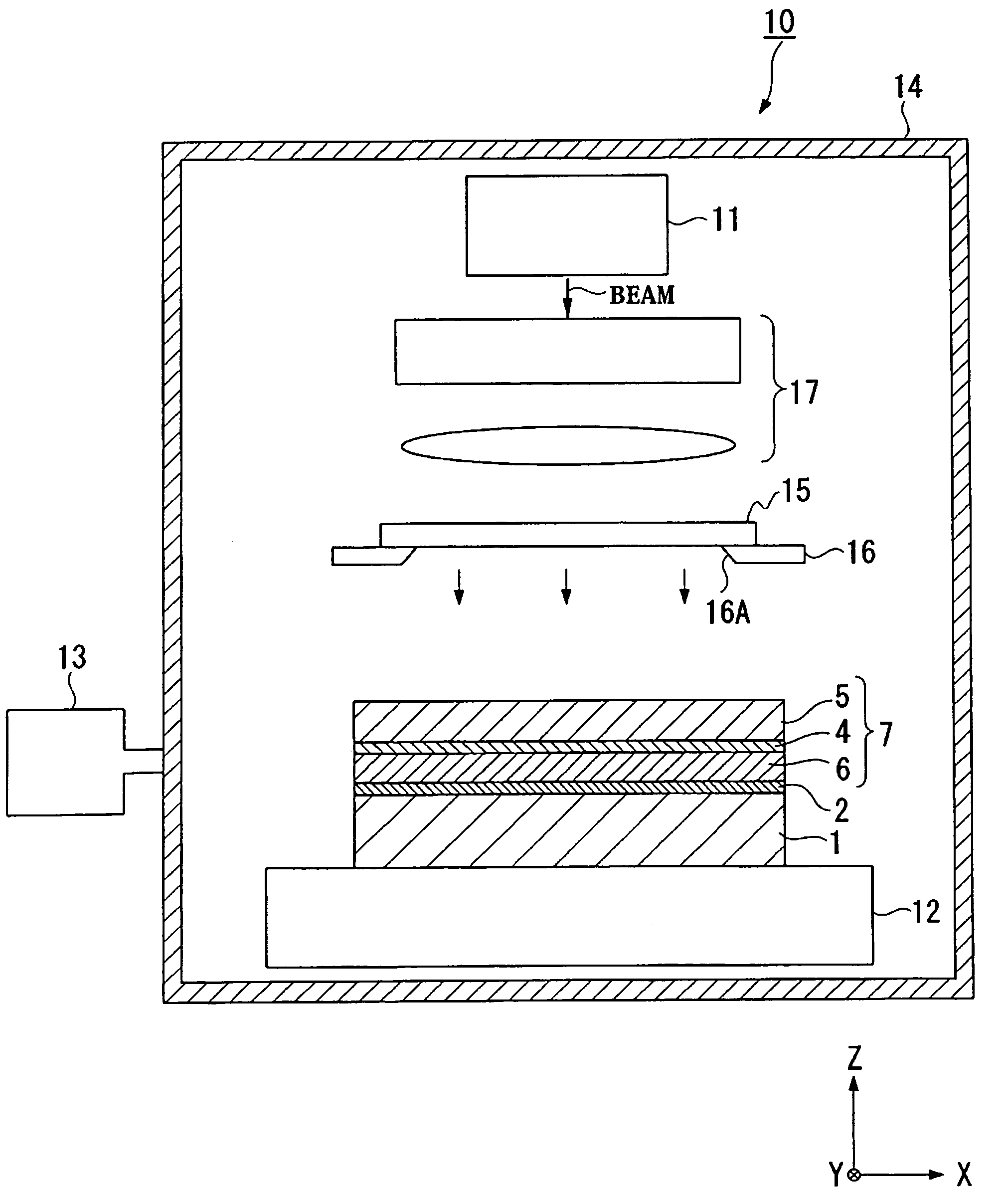
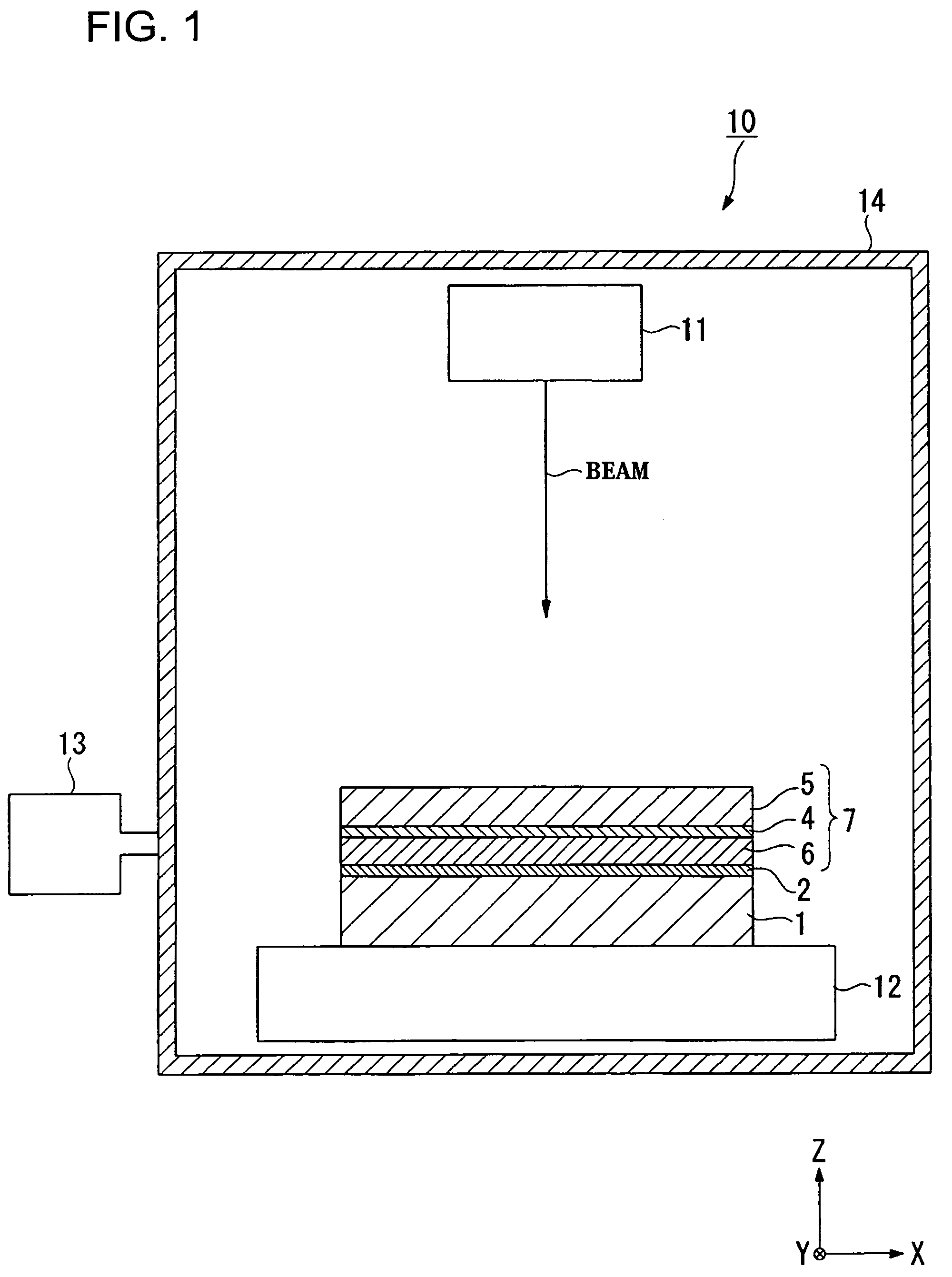
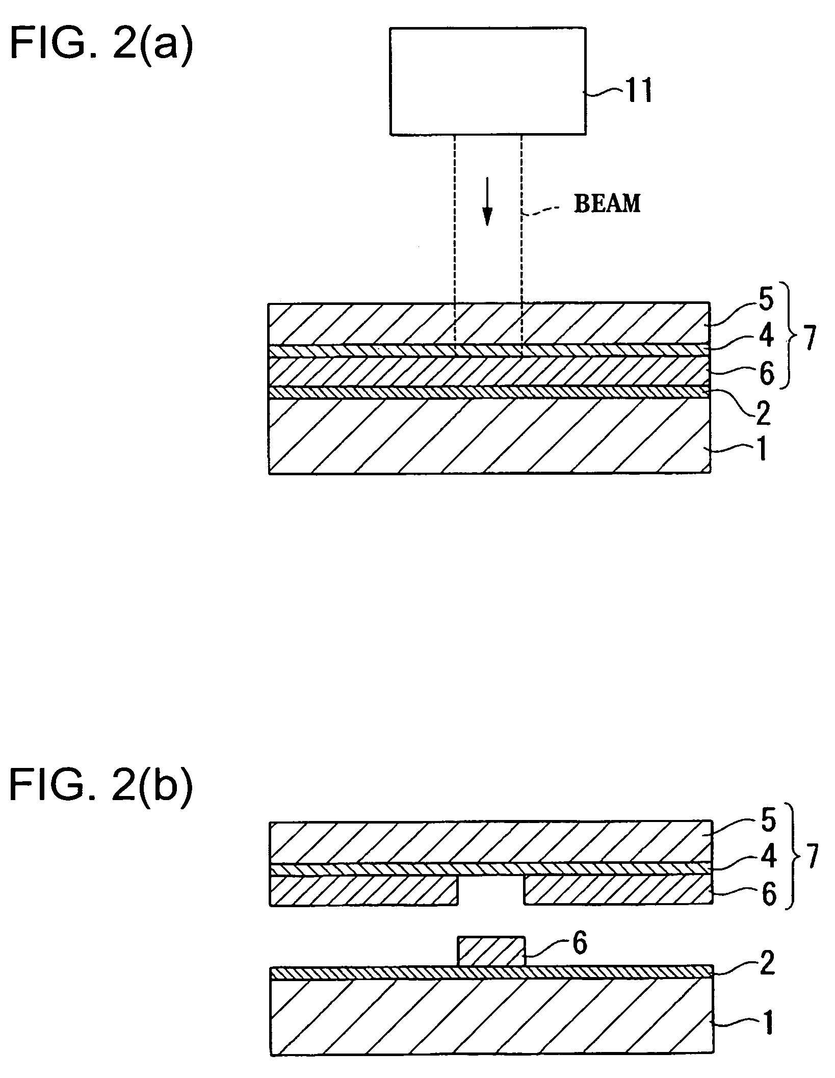
[0039]FIG. 1 is a schematic showing one example of a film-forming apparatus for use in the method to form a film according to exemplary embodiments of the present invention. In FIG. 1, the film-forming apparatus 10 includes a laser beam source 11, which emits a laser beam having a predetermined wavelength and a stage 12, which supports a workpiece 1. The workpiece 1 is treated to have a so-called monomolecular film (surface treatment film) 2 on the surface. The laser beam source 11 and the stage 12, which supports the workpiece 1, are disposed in a chamber 14. The chamber 14 is coupled to an aspirator 13, which can remove gas in the chamber 14. In the present exemplary embodiment, a near-infrared semiconductor laser (wavelength 830 nm) is used as the laser beam source 11.

[0040]In the following descrip...


PUM

PropertyMeasurementUnit
wavelengthaaaaaaaaaa
thicknessaaaaaaaaaa
temperatureaaaaaaaaaa

Abstract

Exemplary embodiments of the invention to provide an efficient and productive method to form a reliable film. A method to form a film according to exemplary embodiments of the present invention, in which a transferring layer formed on a substrate is transferred to a workpiece to form a predetermined film on the workpiece, includes treating a surface of the workpiece to enhance or improve the adhesion between the transferring layer and the workpiece by chemical interaction.

Description

BACKGROUND OF THE INVENTION[0001]1. Field of Invention[0002]Exemplary embodiments of the present invention relate to a method to form a predetermined film on a workpiece, a method to form a wiring pattern using the method to form a film, a method to manufacture a semiconductor device, and to an electro-optical device and an electronic device that have the wiring pattern and / or the semiconductor device.[0003]2. Description of Related Art[0004]The industrial application of a transferring technique utilizing a laser is disclosed in the related art. For example, techniques called laser thermal transfer and laser-induced thermal imaging (LITI) have been adopted. For example, related art Documents Japanese Unexamined Patent Application Publication No. 10-208881 and Japanese Unexamined Patent Application Publication No. 2001-249342 disclose techniques in which transferring layers formed on substrates are transferred to workpieces by laser irradiation.SUMMARY OF THE INVENTION[0005]In such t...

Claims


Application Information

Patent Timeline
Patent Type & Authority Patents(United States)
IPC IPC(8): B44C1/00B32B27/16H01L21/36B29C65/48G01C3/00G03F7/34B05D1/28B05D5/12B05D7/00B32B38/10H01J9/02H01J11/12H01J11/22H01J11/24H01J11/26H01J11/34H01L21/20H01L21/26H01L21/28H01L21/288H01L21/3205H01L21/336H01L21/768H01L29/786H01L51/50H05B33/10H05K3/04H05K3/20H05K3/38
CPCB32B38/10H05K3/046B32B37/025B32B38/0008B32B2310/0843B32B2310/14B32B2457/08H05K3/386H05K3/389H05K2203/0528H05K2203/107H01L21/20H01L21/26H01L21/28
Inventor TOYODA, NAOYUKI
Owner INTELLECTUAL KEYSTONE TECH LLC
Why Eureka
Try Eureka