Method for forming film, method for forming wiring pattern, method for manufacturing semiconductor device, electro-optical device, and electronic device

Active Publication Date: 2005-04-28
INTELLECTUAL KEYSTONE TECH LLC
View PDF12 Cites 53 Cited by
  • Summary
  • Abstract
  • Description
  • Claims
  • Application Information

AI Technical Summary

Benefits of technology

[0019] In the method to form a film according to exemplary embodiments of the present invention, the light may be a laser beam that has a wavelength depending on the light-heat converting material. Thus, the light energy supplied to the light-heat converting material can be efficiently converted into thermal energy.
[0020] In the method to form a film according to exemplary embodiments of the present invention, the light irradiation to the substrate may be performed through a mask having a predetermined pattern. This provides a film pattern having a smaller diameter than the emitted beam. Alternatively, the light irradiation may be performed while moving the substrate and the workpiece relative to the light. In other words, the irradiation light (laser beam) is moved relative to the substrate and the workpiece to pattern the film. This eliminates a step of manufacturing the mask.
[0021] In the method to form a film according to exemplary embodiments of the present invention, the substrate may be exposed to the light while the transferring layer on the substrate is in close contact with the workpiece. This allows the transferring layer to be transferred smoothly from the substrate to the workpiece. In this case, the transferring layer on the substrate is first placed opposite the workpiece. Then, the space between the transferring layer and the workpiece is depressurized, and the transferring layer and the workpiece are brought into close contact with each other. After transferring, the substrate and the workpiece can be separated by relieving the vacuum.
[0022] A method to form a wiring pattern according to exemplary embodiments of the present invention utilizes a film pattern obtained by the method to form a film, serving as a wiring. In other words, the transferring layer (film pattern) formed on the workpiece by the method to form a film can be used for

Problems solved by technology

Decreased adhesive strength between a substrate and a transferring layer may cause the entire transferring layer to be transferred to the workpiece without patterning.
Decreased

Method used


Image

  • Method for forming film, method for forming wiring pattern, method for manufacturing semiconductor device, electro-optical device, and electronic device
  • Method for forming film, method for forming wiring pattern, method for manufacturing semiconductor device, electro-optical device, and electronic device
  • Method for forming film, method for forming wiring pattern, method for manufacturing semiconductor device, electro-optical device, and electronic device

Examples


Embodiment Construction

[0038] Method to Form A Film

[0039] The method to form a film according to exemplary embodiments of the present invention will now be further illustrated with reference to the attached drawings.

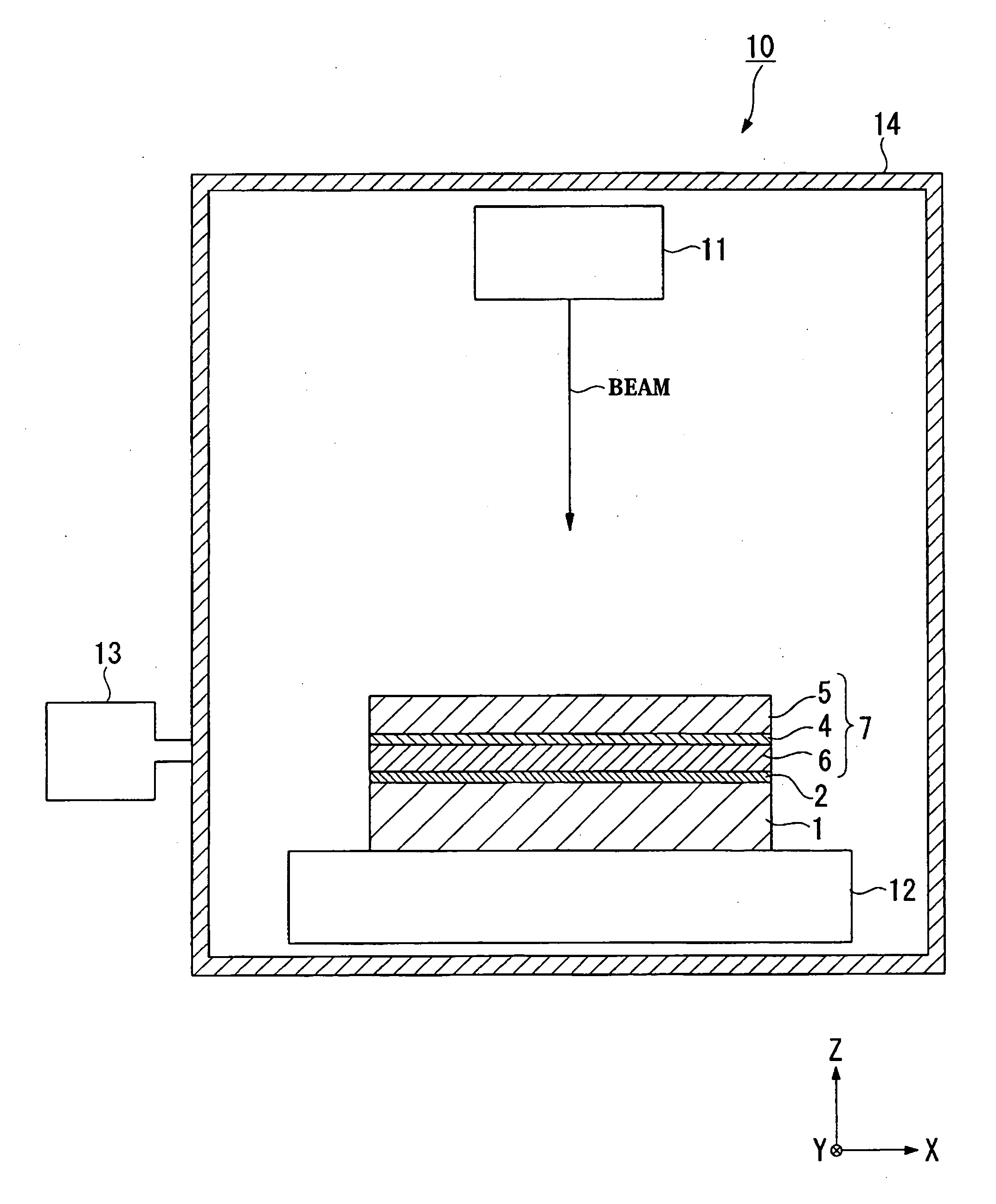
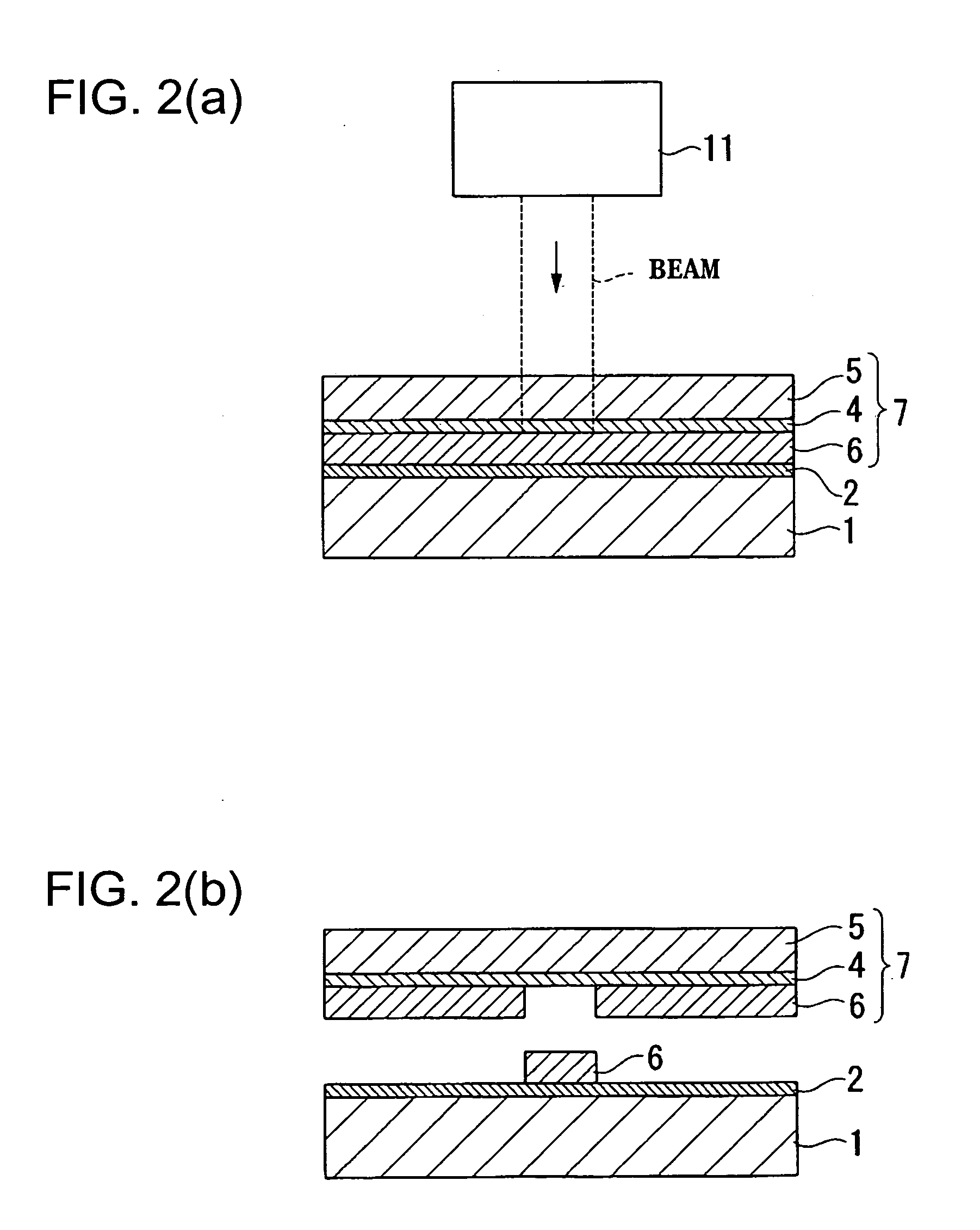
[0040]FIG. 1 is a schematic showing one example of a film-forming apparatus for use in the method to form a film according to exemplary embodiments of the present invention. In FIG. 1, the film-forming apparatus 10 includes a laser beam source 11, which emits a laser beam having a predetermined wavelength and a stage 12, which supports a workpiece 1. The workpiece 1 is treated to have a so-called monomolecular film (surface treatment film) 2 on the surface. The laser beam source 11 and the stage 12, which supports the workpiece 1, are disposed in a chamber 14. The chamber 14 is coupled to an aspirator 13, which can remove gas in the chamber 14. In the present exemplary embodiment, a near-infrared semiconductor laser (wavelength 830 nm) is used as the laser beam source 11.

[0041] In the follo...


PUM

PropertyMeasurementUnit
Adhesion strengthaaaaaaaaaa
Energyaaaaaaaaaa
Hydrophobicityaaaaaaaaaa

Abstract

Exemplary embodiments of the invention to provide an efficient and productive method to form a reliable film. A method to form a film according to exemplary embodiments of the present invention, in which a transferring layer formed on a substrate is transferred to a workpiece to form a predetermined film on the workpiece, includes treating a surface of the workpiece to enhance or improve the adhesion between the transferring layer and the workpiece by chemical interaction.

Description

BACKGROUND OF THE INVENTION [0001] 1. Field of Invention [0002] Exemplary embodiments of the present invention relate to a method to form a predetermined film on a workpiece, a method to form a wiring pattern using the method to form a film, a method to manufacture a semiconductor device, and to an electro-optical device and an electronic device that have the wiring pattern and / or the semiconductor device. [0003] 2. Description of Related Art [0004] The industrial application of a transferring technique utilizing a laser is disclosed in the related art. For example, techniques called laser thermal transfer and laser-induced thermal imaging (LITI) have been adopted. For example, related art Documents Japanese Unexamined Patent Application Publication No. 10-208881 and Japanese Unexamined Patent Application Publication No. 2001-249342 disclose techniques in which transferring layers formed on substrates are transferred to workpieces by laser irradiation. SUMMARY OF THE INVENTION [0005...

Claims


Application Information

Patent Timeline
IPC IPC(8): G03F7/34B05D1/28B05D5/12B05D7/00B32B38/10H01J9/02H01J11/12H01J11/22H01J11/24H01J11/26H01J11/34H01L21/20H01L21/26H01L21/28H01L21/288H01L21/3205H01L21/336H01L21/768H01L29/786H01L51/50H05B33/10H05K3/04H05K3/20H05K3/38
CPCB32B37/025B32B38/0008B32B38/10B32B2310/0843B32B2310/14H05K2203/107H05K3/046H05K3/386H05K3/389H05K2203/0528B32B2457/08H01L21/20H01L21/26H01L21/28
Inventor TOYODA, NAOYUKI
Owner INTELLECTUAL KEYSTONE TECH LLC
Why Eureka
Try Eureka