Pattern forming method and wiring pattern forming method, and electro-optic device and electronic equipment

a technology of pattern forming and pattern forming, which is applied in the direction of diffusion transfer process, thermography, instruments, etc., can solve the problems of difficult patterning, high cost and large-scale device, and the above-mentioned related art, etc., to achieve low cost device structure, high precision, and efficient conversion into thermal energy

Active Publication Date: 2005-02-17
INTELLECTUAL KEYSTONE TECH LLC
View PDF1 Cites 4 Cited by
  • Summary
  • Abstract
  • Description
  • Claims
  • Application Information

AI Technical Summary

Benefits of technology

[0019] In the pattern forming method of the present invention, it is preferable that the light is laser light and has a wavelength according to at least one of the sublimable material and the photothermal conversion material. Thereby, light energy of the light irradiated to the sublimable material or the photothermal conversion material can be efficiently converted into thermal energy. In particular, the use of infrared laser light as the light allows a comparatively low cost device structure to be attained. Furthermore, the light irradiation is preferably performed in such a manner that the light focuses on the sublimable dyestuff layer or the photothermal conversion layer. Thereby, the light energy can be supplied to a desired region of the sublimable dyestuff layer or the photothermal conversion layer with high precision and at a high resolution, thereby forming the thin film pattern at a high resolution conveniently.
[0020] In a wiring pattern forming method of the present invention, a wiring pattern is formed on the base material having the thin film pattern formed by the above-mentioned pattern forming method. Furthermore, the wiring pattern forming method of the present invention comprises a step of arranging a droplet containing a wiring pattern forming material on the base material where the thin film pattern is formed. According to the present invention, based on a droplet discharging method, the fine wiring pattern can be favorably formed at a high resolution while suppressing the loss of consumed materials.

Problems solved by technology

Meanwhile, the above-mentioned related art has a problem described below.
This is because an absorption band of the monomolecular film to be patterned exists in the short wavelength, and with regard to infrared rays of a long wavelength which does not have the absorption band or the like, however high energy light is irradiated, the patterning is difficult.
Therefore, the patterning of an organic thin film such as the monomolecular film has required an expensive large-scaled device such as ultraviolet irradiation and electron beam under vacuum.

Method used


Image

  • Pattern forming method and wiring pattern forming method, and electro-optic device and electronic equipment
  • Pattern forming method and wiring pattern forming method, and electro-optic device and electronic equipment
  • Pattern forming method and wiring pattern forming method, and electro-optic device and electronic equipment

Examples


Embodiment Construction

[0040]

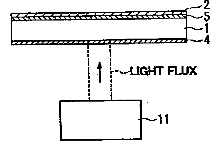
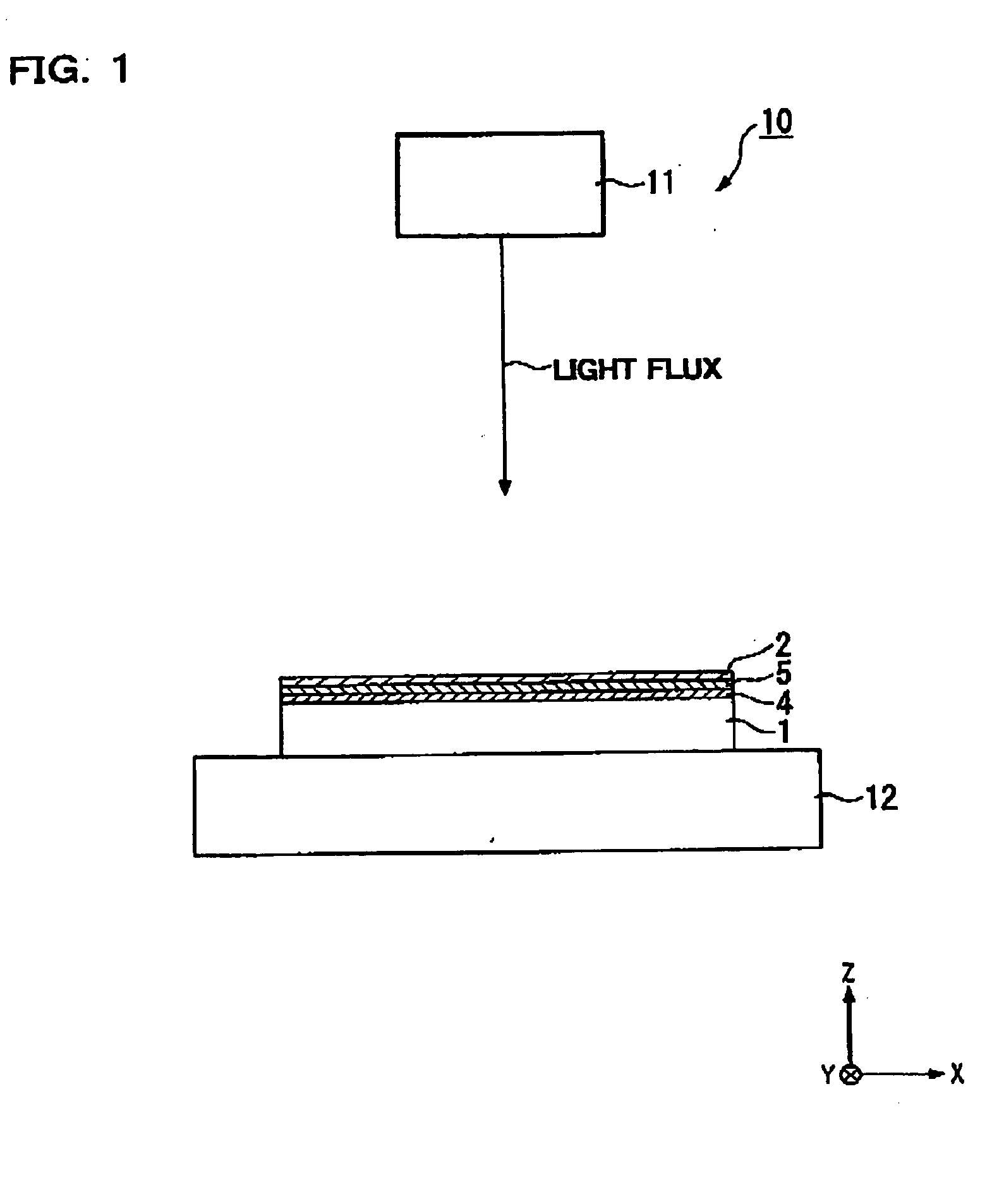
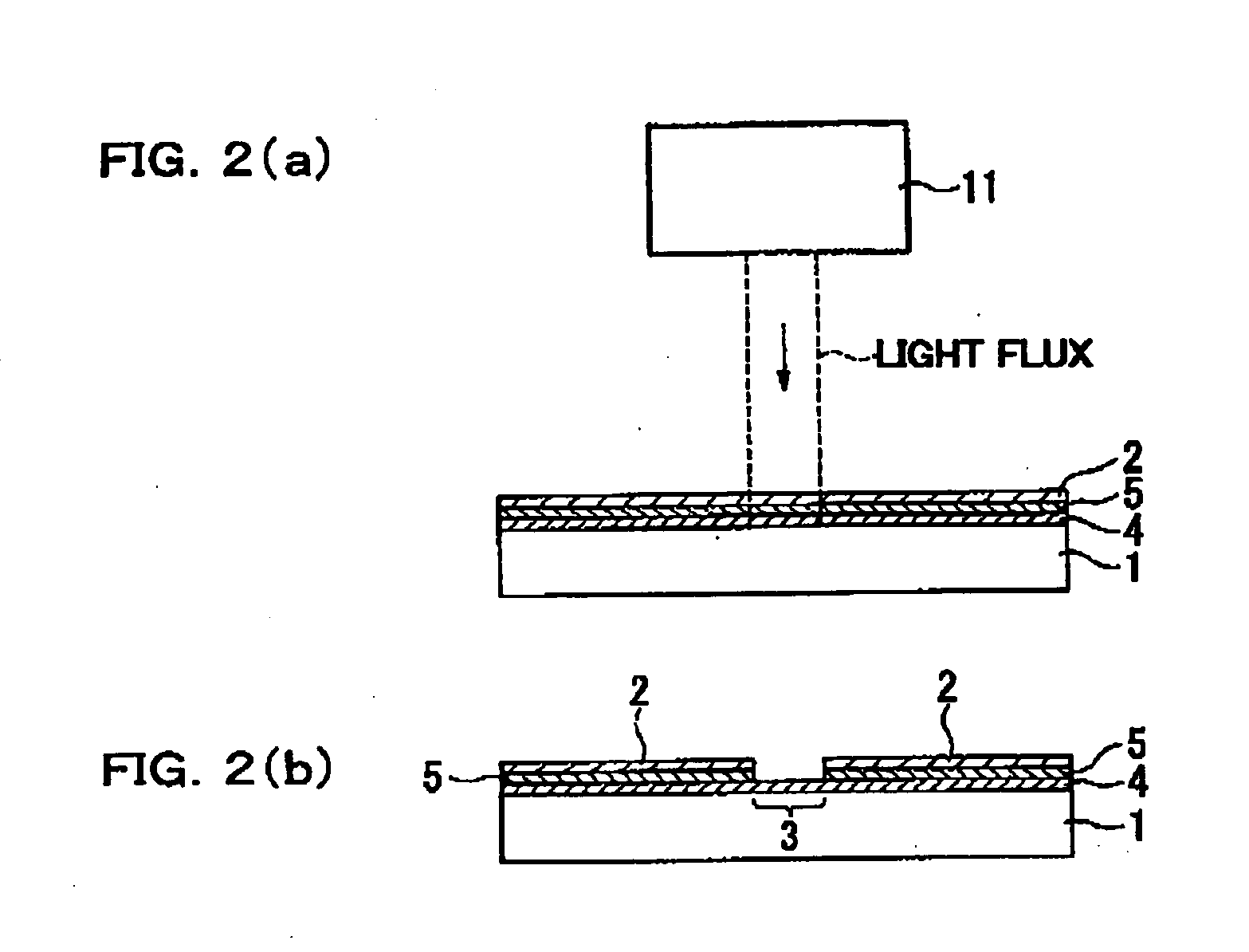
[0041] Hereinafter, a description of a pattern forming method of the present invention is given referring to the drawings. FIG. 1 is a schematic structural view showing one embodiment of a pattern forming device used for the thin film pattern forming method of the present invention. In FIG. 1, a pattern forming device 10 comprises a laser light source 11 emitting laser light flux having a predetermined wavelength, and a stage 12 supporting a base material 1 to be processed. On an upper surface of the base material 1, a photothermal conversion layer 4 is provided, on the photothermal conversion layer 4, a sublimable dyestuff layer 5 is provided, and on the sublimable dyestuff layer 5, a thin film 2 is provided. In this structure (the respective layers on the upper surface side) of the base material 1, it is also possible that the photothermal conversion layer 4 is omitted to provide the sublimable dyestuff 5 on the upper surface of the base material 1, and to provide the thin f...


PUM

PropertyMeasurementUnit
wavelengthaaaaaaaaaa
thicknessaaaaaaaaaa
temperatureaaaaaaaaaa

Abstract

To provide a pattern forming method enabling a thin film to be patterned with high precision by easy and low cost techniques. A thin film 2 is provided on a base material 1 containing a sublimable dyestuff, light is irradiated to the base material 1, and heat generated by the light irradiation sublimates the sublimable dyestuff in a desired region, thereby removing the thin film 2 corresponding to an irradiation region where the light is irradiated to thereby pattern this thin film 2.

Description

BACKGROUND OF THE INVENTION [0001] 1. Field of Invention [0002] The present invention relates to a pattern forming method for forming a thin film pattern on a base material and a forming method of a wiring pattern using the thin film pattern, and an electro-optic device and electronic equipment. [0003] 2. Description of Related Art [0004] Conventionally, as a manufacturing method of a device having a fine wiring pattern such as a semiconductor integrated circuit, a photolithography method is often used, however a device manufacturing method using a droplet discharging method (ink jet method) has attracted attention. There is proposed a method in which in the case where the fine wiring pattern is formed using the droplet discharging method, in order to increase precision in a pattern line width, a liquid repellent region and a lyophilic region are patterned on a base material in advance and a droplet is selectively arranged in the lyophilic region. In Patent Document 1 described belo...

Claims


Application Information

Patent Timeline
Patent Type & Authority Applications(United States)
IPC IPC(8): B05D3/06G03F7/004B05D3/12B41M5/24B41M5/46G02B5/20G02F1/1335G02F1/1343G03C8/00G03F7/00G03F7/36H01L21/20H01L51/00H01L51/50H05B33/10H05B33/14H05B33/26H05K3/06H05K3/14
CPCB41M5/24B41M5/46H01L51/0004B82Y30/00B41M2205/38H10K71/13H01L21/20
Inventor TOYODA, NAOYUKI
Owner INTELLECTUAL KEYSTONE TECH LLC
Why Eureka
Try Eureka