Method for making a semiconductor device with a metal gate electrode that is formed on an annealed high-k gate dielectric layer

a technology of gate dielectric layer and metal gate electrode, which is applied in the direction of semiconductor devices, basic electric elements, electrical appliances, etc., can solve the problems of not being able to apply high-temperature annealing to the high-k dielectric layer, and affecting the performance of the devi

Inactive Publication Date: 2007-05-22
INTEL CORP
View PDF23 Cites 80 Cited by
  • Summary
  • Abstract
  • Description
  • Claims
  • Application Information

AI Technical Summary

Problems solved by technology

MOS field-effect transistors with very thin gate dielectrics made from silicon dioxide may experience unacceptable gate leakage currents.
When, however, a high-k dielectric film is initially formed, it may have a slightly imperfect molecular structure.
If in such a replacement gate process a high-k dielectric layer is formed after a polysilicon layer is removed, it may not be possible to apply a high temperature anneal to the high-k dielectric layer.
It may not be possible to apply such an anneal to such a layer if a silicide has been formed on the transistor's source and drain regions prior to polysilicon layer removal.
In addition, such an anneal may not be feasible if a high temperature intolerant metal has been formed on a first high-k dielectric layer prior to depositing a second high-k dielectric layer.

Method used


Image

  • Method for making a semiconductor device with a metal gate electrode that is formed on an annealed high-k gate dielectric layer
  • Method for making a semiconductor device with a metal gate electrode that is formed on an annealed high-k gate dielectric layer
  • Method for making a semiconductor device with a metal gate electrode that is formed on an annealed high-k gate dielectric layer

Examples


Embodiment Construction

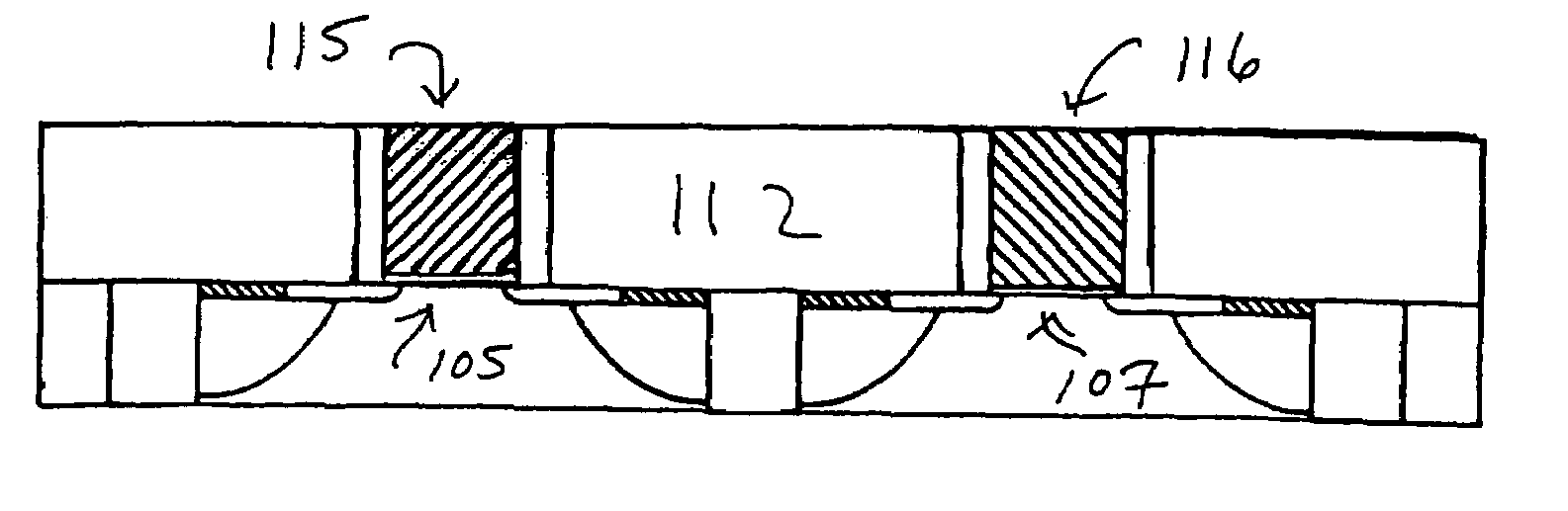
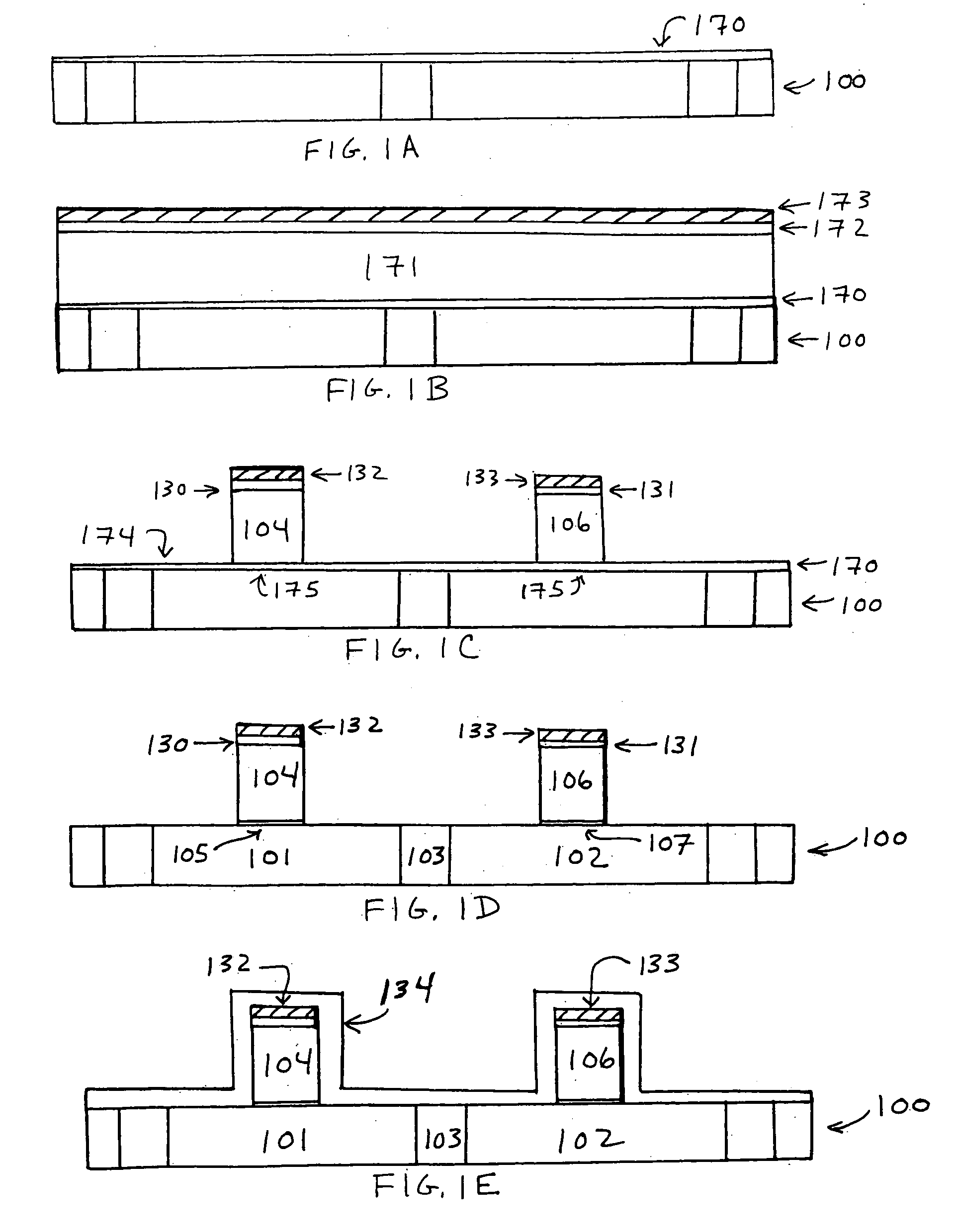
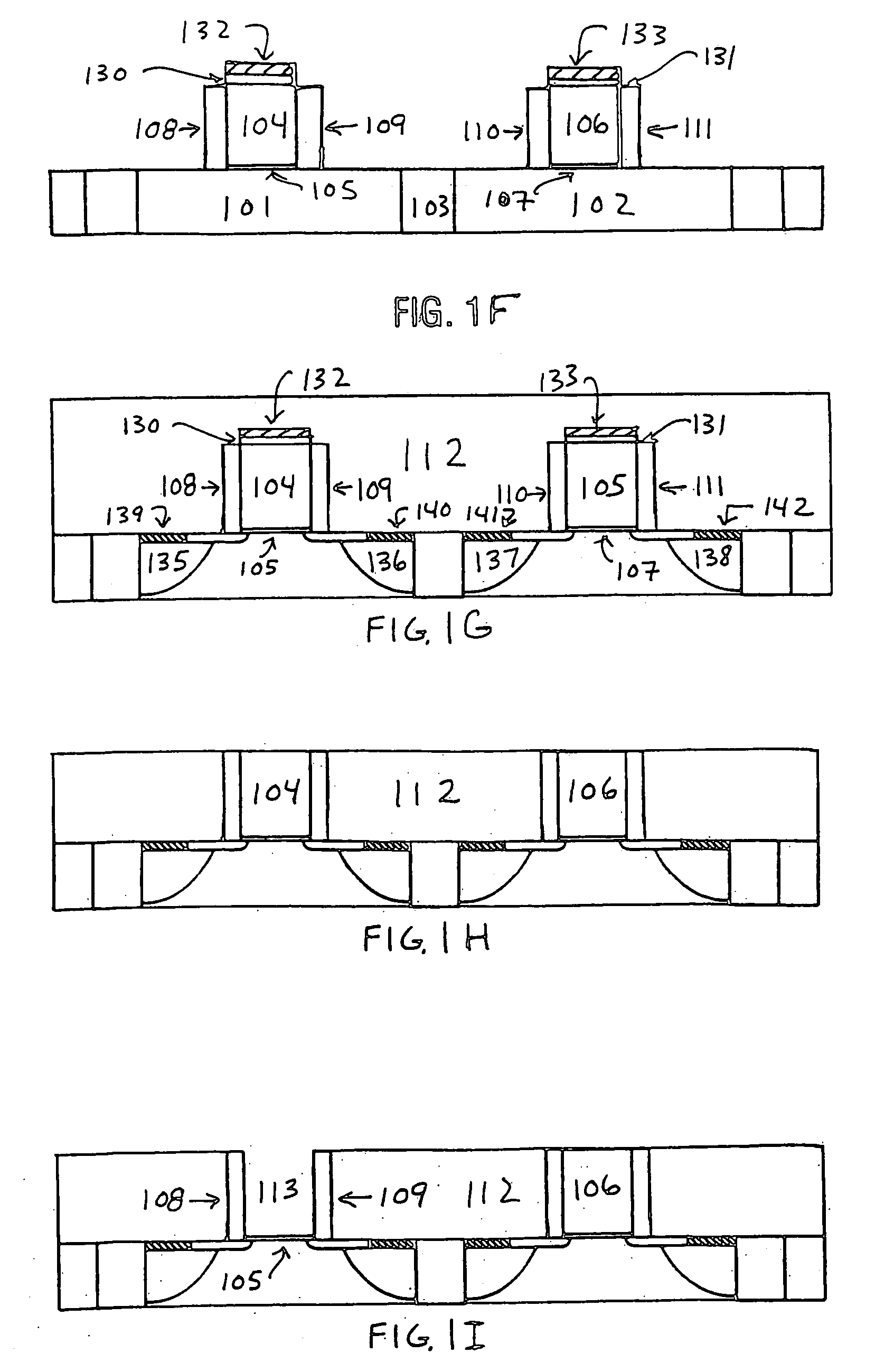
[0009]A method for making a semiconductor device is described. That method comprises forming a high-k gate dielectric layer on a substrate, and forming a sacrificial layer on the high-k gate dielectric layer. After etching the sacrificial layer and the high-k gate dielectric layer to form a patterned sacrificial layer and a patterned high-k gate dielectric layer, first and second spacers are formed on opposite sides of the patterned sacrificial layer. The patterned sacrificial layer is then removed to expose the patterned high-k gate dielectric layer and to generate a trench that is positioned between the first and second spacers. A metal layer is then formed on the high-k gate dielectric layer.

[0010]In the following description, a number of details are set forth to provide a thorough understanding of the present invention. It will be apparent to those skilled in the art, however, that the invention may be practiced in many ways other than those expressly described here. The inventi...


PUM


Abstract

A method for making a semiconductor device is described. That method comprises forming a high-k gate dielectric layer on a substrate, and forming a sacrificial layer on the high-k gate dielectric layer. After etching the sacrificial layer, first and second spacers are formed on opposite sides of the sacrificial layer. After removing the sacrificial layer to generate a trench that is positioned between the first and second spacers, a metal layer is formed on the high-k gate dielectric layer.

Description

FIELD OF THE INVENTION[0001]The present invention relates to methods for making semiconductor devices, in particular, semiconductor devices with metal gate electrodes.BACKGROUND OF THE INVENTION[0002]MOS field-effect transistors with very thin gate dielectrics made from silicon dioxide may experience unacceptable gate leakage currents. Forming the gate dielectric from certain high-k dielectric materials, instead of silicon dioxide, can reduce gate leakage. When, however, a high-k dielectric film is initially formed, it may have a slightly imperfect molecular structure. To repair such a film, it may be necessary to anneal it at a relatively high temperature.[0003]Because such a high-k dielectric layer may not be compatible with polysilicon, it may be desirable to use metal gate electrodes in devices that include high-k gate dielectrics. When making a CMOS device that includes metal gate electrodes, it may be necessary to make the NMOS and PMOS gate electrodes from different materials...

Claims


Application Information

Patent Timeline
Patent Type & Authority Patents(United States)
IPC IPC(8): H01L21/8238
CPCH01L21/28079H01L21/31691H01L21/823842H01L21/823857H01L29/495H01L29/66545H01L29/51H01L21/02197
Inventor BRASK, JUSTIN K.DOCZY, MARK L.KAVALIEROS, JACKSHAH, UDAYMETZ, MATTHEW V.BARNS, CHRIS E.DATTA, SUMANTHOMAS, CHRISTOPHER D.CHAU, ROBERT S.
Owner INTEL CORP
Why Eureka
Try Eureka