Modulator and correction method thereof

a modulator and correction method technology, applied in the field of modulator and correction method thereof, can solve the problems of affecting the modulation accuracy of the modulator, so as to prevent the degradation of the modulation accuracy

Inactive Publication Date: 2007-05-29
PANASONIC CORP
View PDF10 Cites 23 Cited by
  • Summary
  • Abstract
  • Description
  • Claims
  • Application Information

AI Technical Summary

Benefits of technology

[0019]A modulator according to the invention comprises a PLL including a voltage-controlled oscillator, a frequency divider and a phase comparator, the modulator generating a modulating signal based on the modulation data having information on a wider bandwidth than the frequency bandwidth of the PLL, setting the division ratio of the frequency divider by way of this modulating signal, and outputting a modulated carrier signal from the voltage-controlled oscillator as well as performing filtering processing by way of a pre-distortion filter on the modulation data to provide a frequency characteristic inverse to the frequency characteristic of the PLL in a process of generating the modulation signal, thereby allowing wideband modulation, wherein the modulator comprises error detection means for detecting a difference between an amplitude value in a frequency equal to or below the cutoff frequency of the PLL and an amplitude value in a frequency higher than the cutoff frequency concerning an a.c. component of the modulating signal appearing on a control terminal of the voltage-controlled oscillator, and frequency characteristic correction means for correcting at least one of the frequency characteristic of the PLL and the frequency characteristic of the pre-distortion filter in a direction the detected difference is eliminated.
[0020]With this configuration, it is possible to correct the frequency characteristic of a PLL or a pre-distortion filter. This correction eliminates the deviation between the frequency characteristic of the PLL and that of the pre-distortion filter thus providing a flat gain characteristic even in a frequency band exceeding the cutoff frequency of the PLL. As a result, it is possible to prevent degradation in modulation accuracy even in the presence of a variation in the manufacture of circuit components.

Problems solved by technology

However, there is a problem that, broadening the PLL bandwidth fails to suppress a noise from each component of the PLL thus inviting degradation in the noise characteristic.
In reality, it is difficult to obtain a flat gain characteristic in a frequency range exceeding the cutoff frequency of a PLL.
As mentioned earlier, in reality, it is difficult to obtain such a gain characteristic due to a reason such as a variation in the characteristic of circuit components of a PLL.
This prevents a flat characteristic from being obtained, which degrades the modulation accuracy.

Method used


Image

  • Modulator and correction method thereof
  • Modulator and correction method thereof
  • Modulator and correction method thereof

Examples


first embodiment

(First Embodiment)

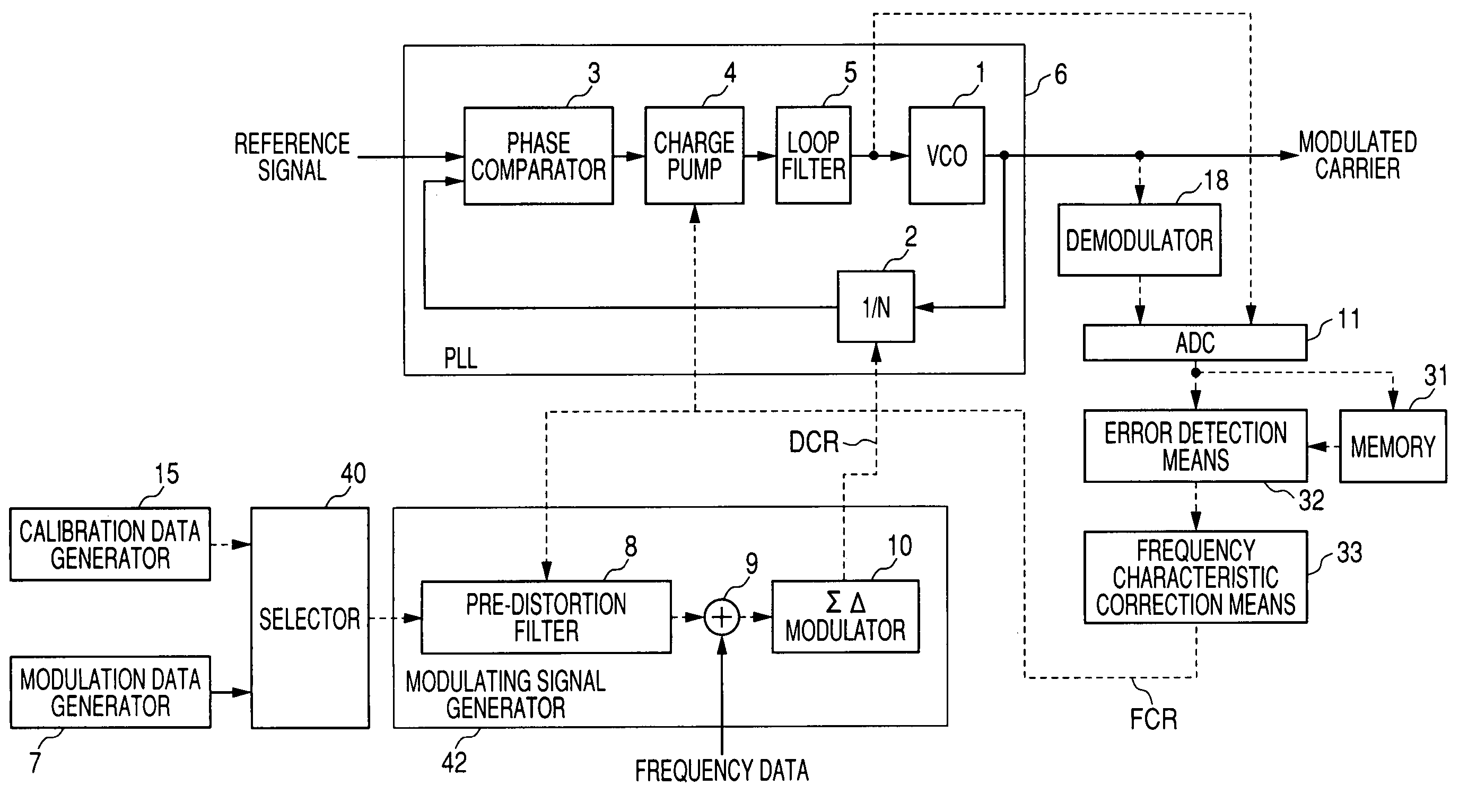
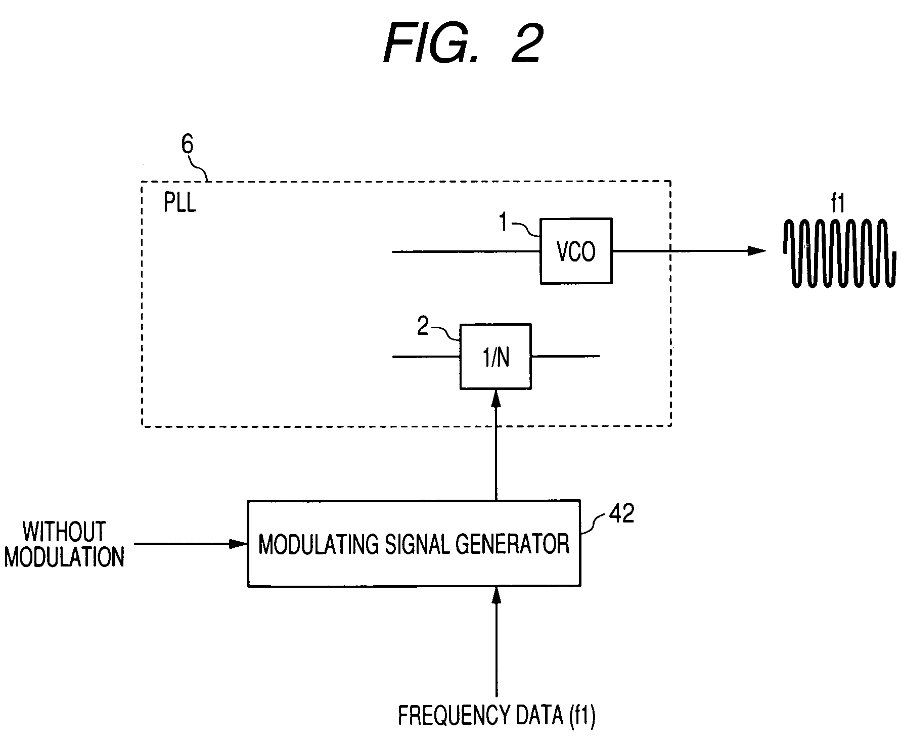
[0073]FIG. 1 is a block diagram showing the configuration of a wideband modulator using a PLL frequency synthesizer according to a first embodiment of the invention. FIGS. 2 and 3 illustrate the operation of calibration in the modulator shown in FIG. 1.

[0074]In the first embodiment, a basic configuration of the invention and its feature are clarified. The modulator according to this embodiment shown in FIG. 1 modulates the division ratio of a frequency divider in a PLL and the modulating signal appears on the control terminal of a VCO, as a result of which a modulated carrier signal is output from the VCO.

[0075]As shown in FIG. 1, a PLL 6 comprises a voltage-controlled oscillator (hereinafter referred to as the VCO) 1, a frequency divider (variable frequency divider having a division ratio of 1 / N, where N is an arbitrary integer for convenience in the example of FIG. 1) 2, a phase comparator 3 for comparing the phase of an output signal of the frequency divider 2 a...

second embodiment

(Second Embodiment)

[0104]FIG. 4 is a block diagram showing the configuration of a wideband modulator using a PLL frequency synthesizer according to a second embodiment of the invention. In the configuration of FIG. 4, same components as those in the FIG. 1 are given same signs and numerals in general.

[0105]A modulator according to the second embodiment uses as an input the output signal of the loop filter 5 and comprises correction means 27 for outputting a control signal for correcting the frequency characteristic. The correction means 27 comprises, for example, an A / D converter (ADC) 11 for converting an analog signal to a digital value, a register 12 for storing the output signal of the A / D converter 11, comparison means 13 for comparing the data stored in the register 12 with the output signal of the A / D converter 11, and a filter characteristic control means 14 for controlling the characteristic of the pre-distortion filter 8 based on the output signal of the compassion means 1...

third embodiment

(Third Embodiment)

[0128]FIG. 9 is a block diagram showing the configuration of a wideband modulator using a PLL frequency synthesizer according to a third embodiment of the invention.

[0129]The third embodiment comprises a charge pump current control means for controlling the current gain of a charge pump 4 in accordance with the output of the comparison means 13 instead of a filter characteristic control means 14. In this case, the charge pump 4 is a current output type. Other components are same as those in the second embodiment shown in FIG. 4.

[0130]In the third embodiment, a calibration data generator 15 outputs a signal having a frequency (fBW in this example) corresponding to the modulation bandwidth as shown in FIG. 6. Comparison means 13 compares the output of an A / D converter 11 and that of a register 12 and outputs a comparison result, same as the second embodiment.

[0131]Varying the current gain of the charge pump 4 can vary the frequency characteristic of a PLL 6. Charge p...


PUM


Abstract

The invention concerns a wideband modulator using a PLL synthesizer, which can match the frequency characteristic and prevent degradation in modulation accuracy even in the presence of a variation in the manufacture of circuit components. In a wideband modulator which modulates the division ratio of a frequency divider by using a modulating signal generated by a modulating signal generator and outputs a modulated carrier signal from a VCO, calibration data from a calibration data generator are input via a selector. The amplitude value of an ac component of each modulating signal, either appearing on the output of a loop filter or demodulated by a demodulator, is converted to a digital value by way of an A / D converter. The difference between the two is detected and a control signal FCR to eliminate the difference is generated in order to correct the frequency characteristic of a PLL or a pre-distortion filter.

Description

TECHNICAL FIELD[0001]The present invention relates to a modulator which is used in a radio unit and which generates and outputs a modulated carrier signal in a wider frequency range than a frequency range of a PLL thus performing wideband modulation using a PLL frequency synthesizer, and a correction method therefor.BACKGROUND OF THE INVENTION[0002]In general, a modulator circuit using a PLL synthesizer is required to be low cost, low power consumption as well as good noise characteristic and modulation accuracy. In PLL-based modulation, to provide a better modulation accuracy, it is desirable to provide a wider frequency range of a PLL (PLL bandwidth) rather than a frequency range of a modulating signal (modulation bandwidth). However, there is a problem that, broadening the PLL bandwidth fails to suppress a noise from each component of the PLL thus inviting degradation in the noise characteristic.[0003]In the related art, a technique is described in U.S. Pat. No. 6,008,703, which ...

Claims


Application Information

Patent Timeline
Patent Type & Authority Patents(United States)
IPC IPC(8): H03C3/00H04L27/20H03L7/06H03C1/00H03C3/09H03L7/093H03L7/183H03L7/197
CPCH03C3/0925H03C3/0933H03C3/0991H03L7/1976
Inventor HIRANO, SHUNSUKEMIYAHARA, YASUNORI
Owner PANASONIC CORP
Why Eureka
Try Eureka