Method and device used for eliminating image overlap blurring phenomenon between frames in process of simulating CRT impulse type image display

a technology of image display and image overlap, applied in the field of method and device used to eliminate the image overlap blurring phenomenon between frames in the process of simulating crt impulse type image display, can solve the problems of pixel only producing light, drawbacks and limitations that must be overcome and improved, and much lower power consumption and heat dissipation, so as to reduce the accumulated liquid crystal optical response and eliminate the image overlap blurring phenomenon. , the effect of reducing the luminance of backligh

Inactive Publication Date: 2007-05-29
VASTVIEW TECH
View PDF9 Cites 5 Cited by
  • Summary
  • Abstract
  • Description
  • Claims
  • Application Information

AI Technical Summary

Benefits of technology

[0022]Therefore, the purpose of the present invention is to provide the method and device used for the eliminating the image overlap blurring phenomenon between frames in the process of simulating CRT impulse type image display, so as to solve and overcome the shortcomings and limitations of the above-mentioned related prior art It controls and reduces the accumulated liquid crystal optical response during that interval to the lowest value desired by means of providing scanning black lines on the screen, and coupled with the reduction of backlight luminance to the appropriate low level, thus achieving for certain the purpose of simulating CRT impulse type image display. And by doing so, the present invention can effectively eliminate the phenomenon of image overlap blurring of the “after image” between frames. And as such, the present invention can significantly improve the image displaying quality of the LCD display, in addition to saving the extra cost and expense of the additional equipment.
[0028]Summing up the above, the dotted line (c) in FIG. 2(a) indicates the liquid crystal optical response curve (c) generated by the black line scanning as utilized in the above-mentioned another pending patent application of the present inventor, and curve (d) is the liquid crystal optical response resulting from lowering the luminance response of the backlight unit to the lowest value through the design of the present invention. And by adding the liquid crystal molecule optical response at point “a” in FIG. 2(a), to the backlight luminance response at point “e” in FIG. 2(c), then we can obtain the accumulated liquid crystal response at point “b” in FIG. 2(a). And this is the lowest accumulated liquid crystal optical response generated by the method and device of the present invention, and it can be designed to reach the sufficiently low level according to the quality and effect of the actual liquid crystal image display desired to attain, and achieving for certain the purpose of eliminating the “after image” overlap blurring between frames on the display screen.
[0030]And it must be re-emphasize here that, the lowest value of the liquid crystal accumulated optical response generated by the above-mentioned backlight luminance adjust and control process, is not limited to occur at certain point on the response curve. And the length of the temporal continuation of the lowest value of backlight luminance response can be adjusted by controlling the duration of the applied backlight voltage, so as to enable the lowest value of the liquid crystal molecule optical response to continue for an adjustable interval (for example, the portion of the horizontal linear section between time points A3 and A4 and between time points A6 and A7 as shown in FIG. 2(a)). And as such, it can achieve for certain the purpose and effect of eliminating the “after image” overlap blurring between frames. Therefore, in the above-mentioned FIG. 2(c), time point is used to illustrate the lowest point of the backlight luminance response; its purpose is only for simplifying the explanation and facilitating the understanding.
[0031]In addition, the advantage of backlight units made with LED or EL being superior to those made with CCFL are: its luminance response is of the immediate-target-value mode, and it can immediately reach the nominal luminance target response value as shown in FIG. 2(d). Besides, the backlight units made with LED or EL material can have a plurality of sequentially incrementing nominal target values, which can be applied to different designs. However, as for the backlight unit made with CCFL, its luminance response is slower as the gradual-target-value mode as shown in FIG. 2(c), and it must take a certain period of time to reach the nominal luminance target response value after the backlight unit being applied the control voltage. Therefore, its contribution to the temporal width of reducing the liquid crystal accumulated optical response to the lowest value is smaller. Besides, in general, the luminance response of CCFL made with one kind of material usually has one nominal target value.
[0033]The present invention also relates the method used for eliminating the image overlap blurring between frames in the process of simulating CRT impulse type image display.

Problems solved by technology

The flat display effect of LCD is apparently superior to the image display effect of CRT, and in addition, its power consumption and its heat dissipation are much lower than those of the similar size CRT display.
In addition, for the LED utilized widely at present, which is subject to the limitations in various practical applications due to its inherent characteristics, such as, the LED is preferably used in the static display for numbers, characters, or images, and is not comparable to and can not match the LCD technology which is capable of dynamic image display and be able to achieve the effect of liveliness and vividness.
However, in the liquid crystal display technology of the present days there still exist drawbacks and limitations that must be overcome and improved.
However, the pixel only produces the emission of light in an instant of a minute portion of time in each frame period.
Nevertheless, due to the limitation of the intrinsic property of the liquid crystal material, the image it displays occupies the predominant portion of time of that frame.
However, even the LCD display device made with this kind of over drive technology is able to shorten its gray level response time to less than and within one frame period, yet due to the intrinsic property of the liquid crystal, the generation of its optical response is slow so is its decline.
Therefore, the image overlapping and the image outlines blurring phenomenon of the “after image” for the images displayed still can not be eliminated completely.
However, the three above-mentioned methods have the following drawbacks and limitations, therefore their effects are not ideal, so that the “after image” overlap blurring phenomenon between frames still exists on the LCD screen: (1) necessitating the extra cost and expense of the additional equipment of frequency doubling device or backlight blinking equipment; (2) the electric magnetic interference incurred by the addition of such equipments; (3) for certain liquid crystal materials, their optical responses are fast from brightness to dark, and are slow from dark to brightness; but for other liquid crystal materials their optical responses are slow from brightness to dark, and are fast from dark to brightness.
However, for certain liquid crystal material its optical response is slower from brightness to dark, and during the black line scanning interval its optical response has not yet reached the sufficiently low value.
As such, some of them still result in the phenomenon of certain “after image” overlap blurring.

Method used


Image

  • Method and device used for eliminating image overlap blurring phenomenon between frames in process of simulating CRT impulse type image display
  • Method and device used for eliminating image overlap blurring phenomenon between frames in process of simulating CRT impulse type image display
  • Method and device used for eliminating image overlap blurring phenomenon between frames in process of simulating CRT impulse type image display

Examples


embodiment 1

[0059]In the following analysis, please refer to FIGS. 1, 3(a), 3(b) and 4(a)-4(e) as we explain first embodiment of the present invention.

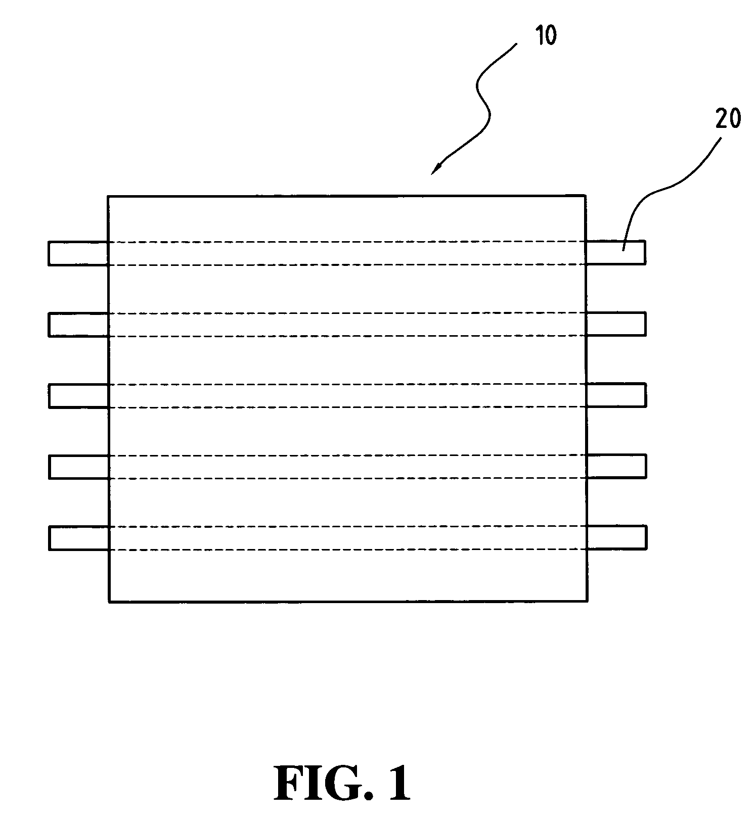
[0060]Referring to FIG. 1, it indicates the structure arrangement of the liquid crystal display panel and backlight unit used according to the first embodiment of the present invention.

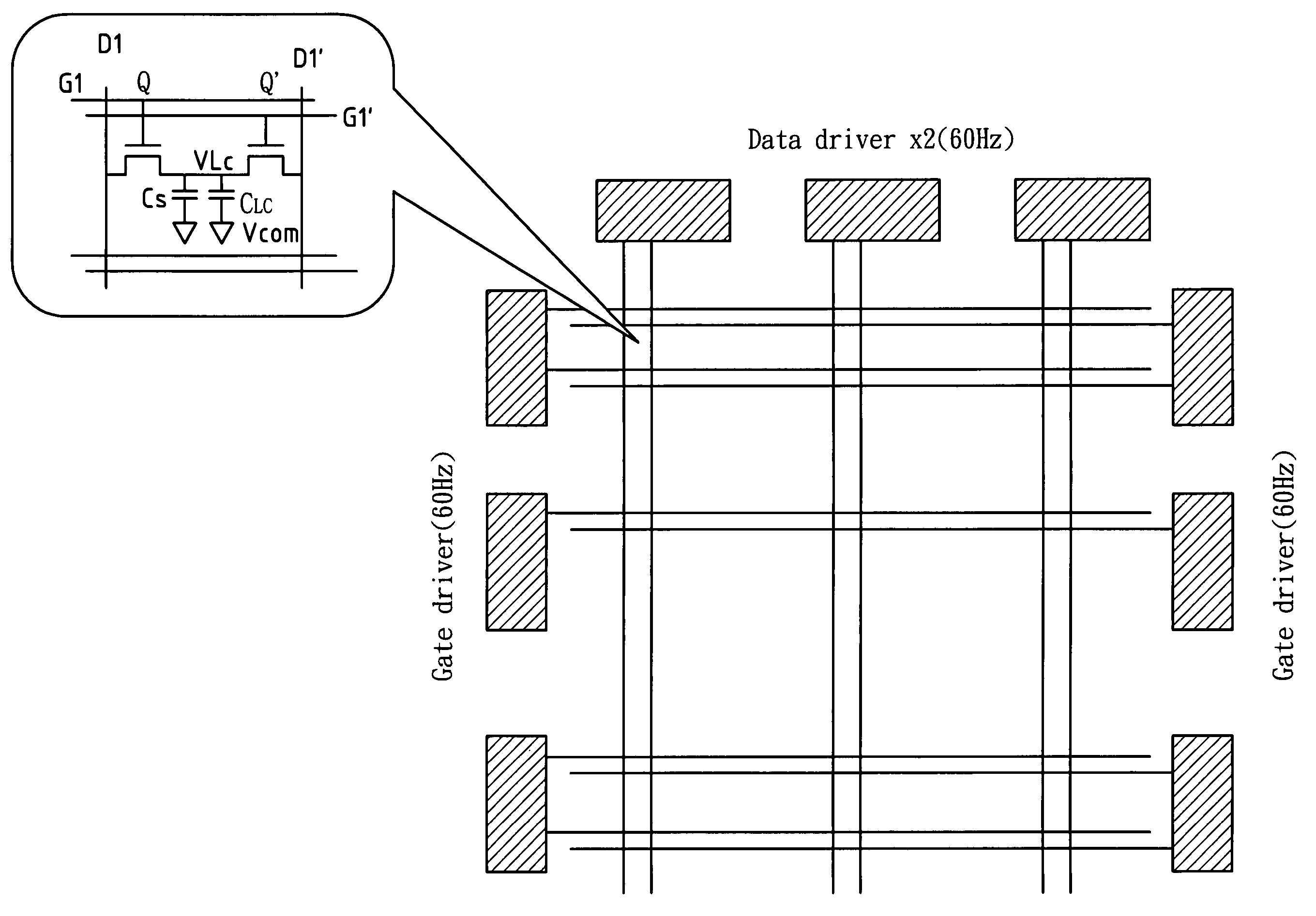
[0061]FIG. 3(a) indicates the pixel array formed by the cross points of a plurality of gate lines and data lines, and the simulation driving circuit formed by a plurality of data driver and gate driver according to the first embodiment of the present invention.

[0062]FIG. 3(b) represents the liquid crystal display simulation driving device according to the first Embodiment.

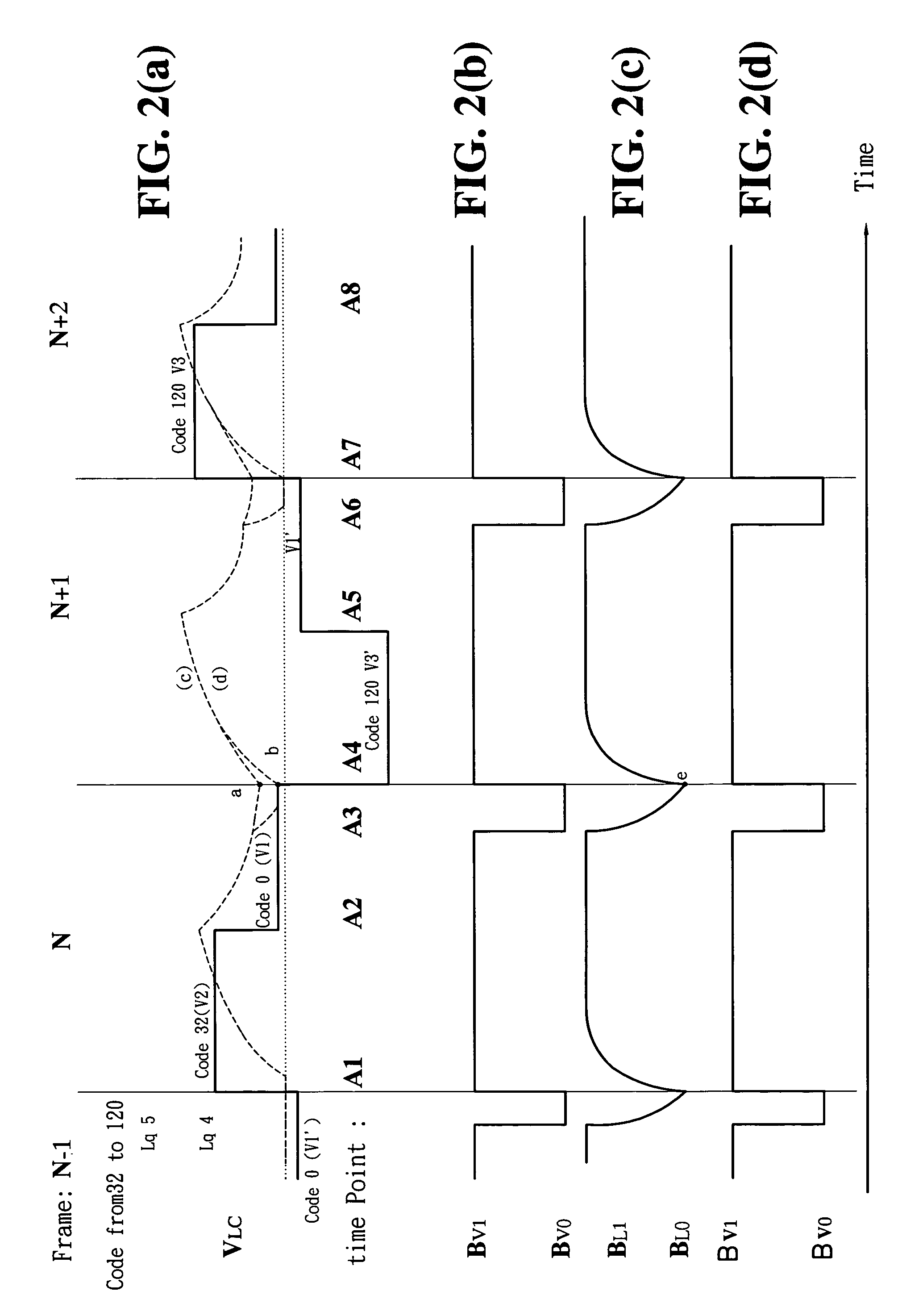
[0063]FIGS. 4(a)-4(d) indicate the relations of the waveform curves between the driving voltage pulse of the liquid crystal molecules VLC, the backlight control voltage BV, backlight luminance response BL, and the accumulated liquid crystal optical response Lq generated by the image blurring elimi...

embodiment 2

[0080]In the following analyses, please refer to FIGS. 1, 5(a), 5(b) and (a) to 6(d) as we explain second embodiment of the present invention.

[0081]First, please refer to FIG. 1, it indicates the structure arrangement of the liquid crystal display panel and backlight unit used according to the second embodiment of the present invention.

[0082]FIG. 5(a) indicates the pixel array formed by the cross points of a plurality of gate lines and data lines, and the simulation driving circuit formed by a plurality of data driver and gate driver according to the second embodiment of the present invention.

[0083]FIG. 5(b) represents the liquid crystal display simulation driving device according to the second embodiment.

[0084]FIGS. 6(a) to 6(d) indicate the relations of the waveform curves between the driving voltage pulse of the liquid crystal molecules VLC, the backlight control voltage BV, backlight luminance response BL, and the accumulated liquid crystal optical response Lq generated by the i...

embodiment 3

[0091]In the following analyses, please refer to FIGS. 1, 7(a), 7(b) and 8(a) to 8(d) as we explain third embodiment of the present invention.

[0092]First, please refer to FIG. 1, its indicates the structure arrangement of the liquid crystal display panel and backlight unit used according to the third embodiment of the present invention.

[0093]FIG. 7(a) indicates the pixel array formed by the cross points of a plurality of gate lines and data lines, and the simulation driving circuit formed by a plurality of data driver and gate driver according to the third embodiment of the present invention.

[0094]FIG. 7(b) represents the liquid crystal display simulation driving device according to the third embodiment.

[0095]FIGS. 8(a) to 8(d) indicate the relations of the waveform curves between the driving voltage pulse of the liquid crystal molecules VLC, the backlight control voltage BV, backlight luminance response BL, and the accumulated liquid crystal optical response Lq generated by the ima...


PUM


Abstract

Disclosed is a device for eliminating after image overlap blurring phenomenon between frames in the simulation of CRT impulse type image display with liquid crystal display (LCD), including first and second input control lines; first and second input data lines; first and second capacitors; a driving voltage output line; a first transistor including a first gate connected to a first input control line, a first source connected to a first input data line, and a first drain connected to a driving voltage output line, a first capacitor and the drain of the second transistor; and a second transistor including a second gate connected to a second input control line, a second source connected to a second input data line, and a second drain connected to a driving voltage output line, the drain of the first transistor and the second capacitor. The first and second capacitors are connected to ground respectively. The driving voltage output line supplies a simulation driving voltage to pixels of an LCD panel for displaying images and including a backlight unit with adjustable and controllable luminance and a backlight input voltage control line. The first and second input control lines are connected to a gate driver. The first and second data lines are connected to a data driver respectively. During the interval of black lines scanning, when the luminance of the backlight unit is reduced to the lowest value through its control voltage, the accumulated liquid crystal optical response in that interval is brought to the lowest value.

Description

BACKGROUND OF THE INVENTION[0001]1. Field of the Invention[0002]The present invention relates to the method and device used for eliminating the image overlap blurring phenomenon between frames in the process of simulating CRT impulse type image display, and more particularly, to the method and device used for eliminating the after image overlap blurring phenomenon between frames in the process of simulating CRT impulse type image display with liquid crystal display (LCD).[0003]2. The Prior Arts[0004]In recent years, liquid crystal display (LCD) device have been very popular and widely used, and the varieties of its products are enormous, from the consumer electronic products to computers and the mobile phone wireless communication applications, such that the technology progress and development of the LCD device is rapidly advancing, and its trend is in agreement with the future trend of the development of the electronic products toward the features of light weight, thin thickness, s...

Claims


Application Information

Patent Timeline
Patent Type & Authority Patents(United States)
IPC IPC(8): G09G3/36
CPCG09G3/3648G09G3/3659G09G3/3677G09G3/3688G09G3/3406G09G3/3614G09G2310/061G09G2310/066G09G2320/0252G09G2320/0261
Inventor CHEN, CHENG-JUNGSHEN, YUH-REN
Owner VASTVIEW TECH
Why Eureka
Try Eureka