Display device and method of driving the same

a technology of display device and drive mechanism, which is applied in the direction of static indicating device, identification means, instruments, etc., can solve the problems of large reduction of voltage, insufficient reverse bias application, and large reduction of luminance of organic light emitting element with time, so as to prevent the reduction of luminance of organic light emitting element and improve the quality of displayed images

Inactive Publication Date: 2007-06-12
SEMICON ENERGY LAB CO LTD
View PDF30 Cites 41 Cited by
  • Summary
  • Abstract
  • Description
  • Claims
  • Application Information

AI Technical Summary

Benefits of technology

[0029]The present invention has been made in view of the above and an object of the present invention is therefore to provide a display device and driving method thereof, in order that an organic light emitting element is driven by applying alternating current voltage to prevent reduction in luminance of the organic light emitting element and the quality of displayed images are improved.
[0039]The circuit shown in FIG. 17 is merely an example of the present invention, and the conductivity of the current controlling TFT 102, the rectifying direction of the rectifying element 109, and the rectifying direction of the organic light emitting element 105 that has the diode structure can be set freely as long as the effects of the present invention are obtained.
[0041]However, it is generally preferred to employ the driving method of FIG. 18B in which the electric potential of an opposite electrode and the electric potential of a power supply line are both changed. The amplitude of voltage outputted from an alternating current source is smaller in the driving method of FIG. 18B than in the driving method of FIG. 18A and therefore the method of FIG. 18B is capable of reducing the cost of alternating current source by using a low-voltage driving alternating current source. When the amplitude of voltage of an alternating current source is smaller, load on circuits that constitute the alternating current source is reduced to improve the reliability of the alternating current source. Furthermore, it is also advantageous in terms of reduction of cost to require less power supply systems in total.

Problems solved by technology

Accordingly, a great reduction in voltage occurs here since the gate electric potential of the current controlling TFT is low, and therefore only insufficient reverse bias is applied to the organic light emitting element.
It is thus difficult to drive an organic light emitting element with alternating current in the conventional circuit structure described above, and the problem of great reduction in luminance of an organic light emitting element with time due to application of direct current voltage is yet to be solved.

Method used


Image

  • Display device and method of driving the same
  • Display device and method of driving the same
  • Display device and method of driving the same

Examples


embodiment mode 1

[Embodiment Mode 1]

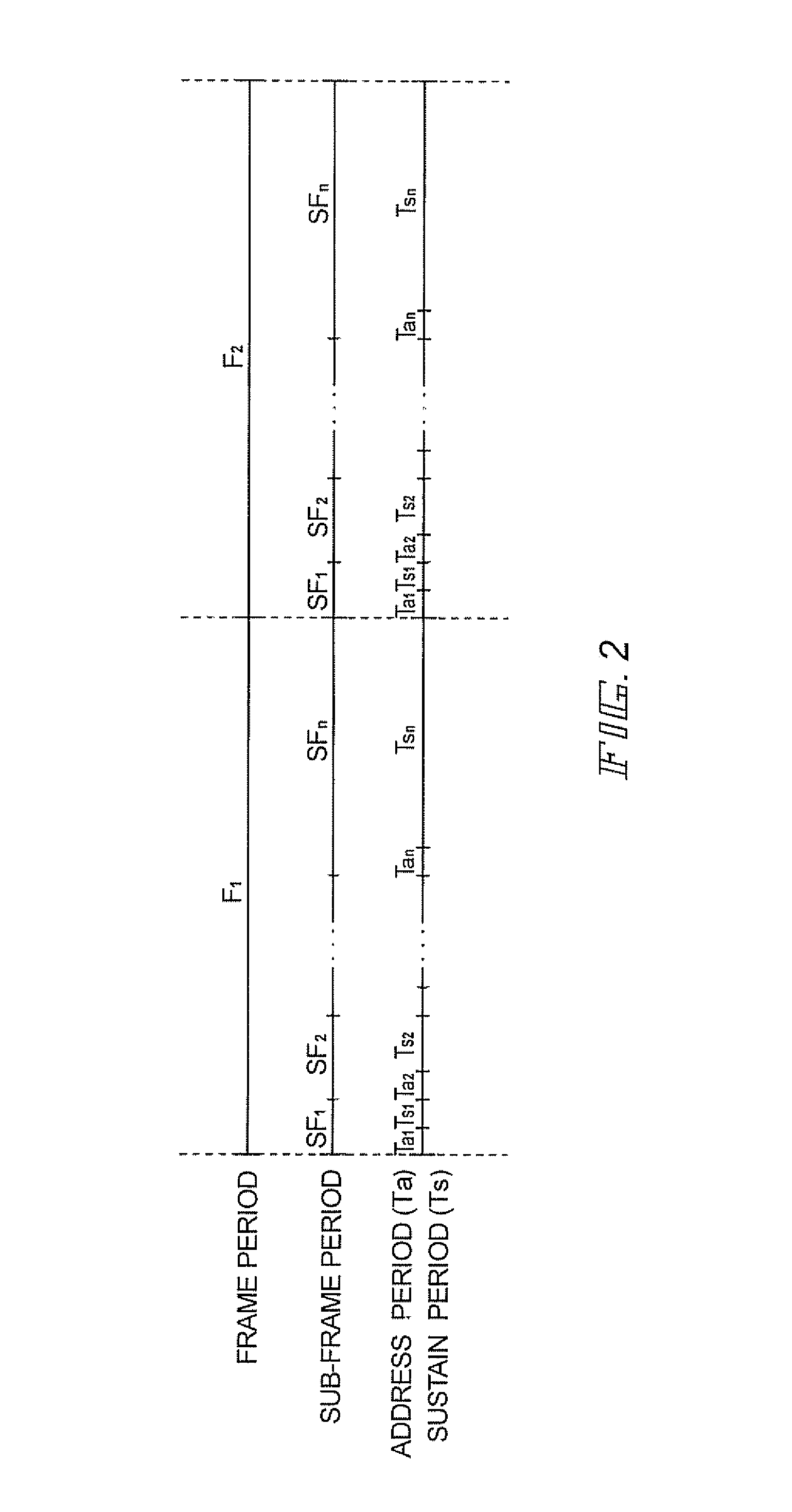
[0097]Described here is an example of applying the structure of the present invention to an organic light emitting display in which gray scale display is performed through time division driving. The gray scale display through time division driving is a method of gray scale display in which gray scales of pixels are controlled by combining several periods that have different time for light emission.

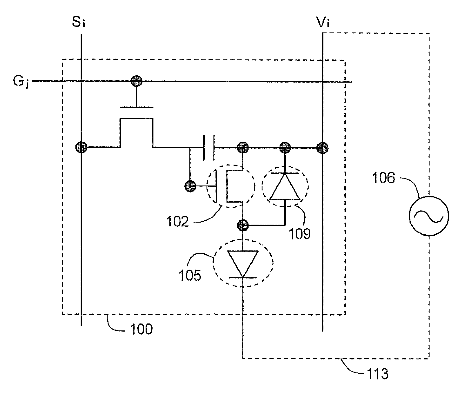
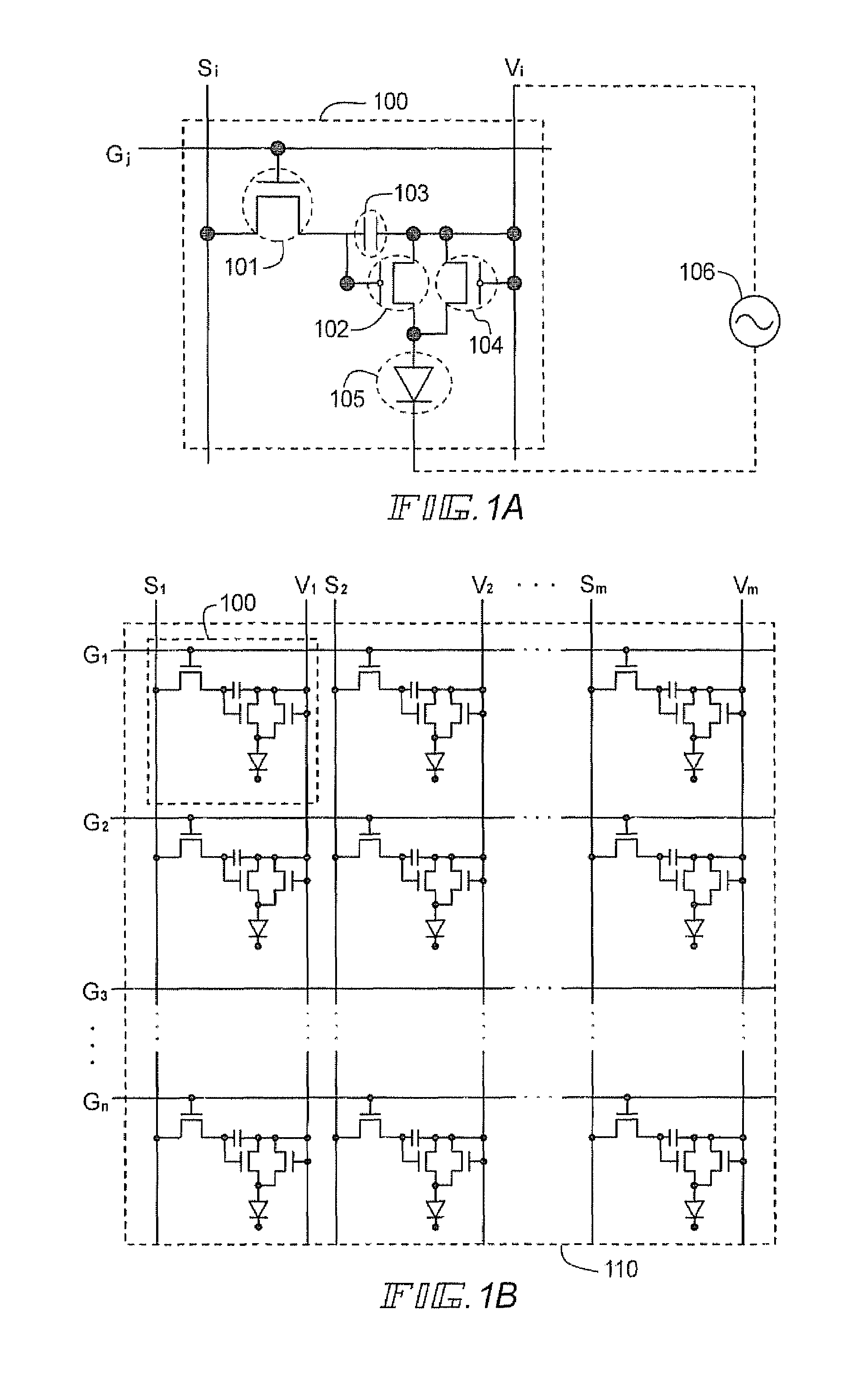
[0098]FIG. 1A is an equivalent circuit of a pixel. Each pixel is denoted by 100 and receives signals from a gate signal line (Gj) and a source signal line (Si). Each pixel has a switching TFT 101, a current controlling TFT 102, a capacitor 103, a rectifying TFT 104, and an organic light emitting element 105. An alternating current source 106 gives electric potentials to a power supply line (Vi) and an opposite electrode of the organic light emitting element 105.

[0099]A gate electrode of the switching TFT 101 is connected to the gate signal line (Gj) for inputting a selec...

embodiment mode 2

[Embodiment Mode 2]

[0137]In a color organic light emitting display, a material of a light emitting layer may differ among a pixel that emits red light, a pixel that emits blue light, and a pixel that emits green light, and the relation between the voltage applied to the organic light emitting element and the intensity of light emitted from the organic light emitting element may vary among pixels of different colors. In this case, one of the electric potential of power supply line and the electric potential of opposite electrode may vary among pixels of different colors.

[0138]For example, a driving method of an organic light emitting display, as illustrated in the waveform of FIG. 4, can be employed. The diagram show electric potentials given by an alternating current source to a power supply line and to an opposite electrode of an organic light emitting element. The electric potential of the power supply line varies in accordance with the color of light emitted from a pixel. The axi...

embodiment mode 3

[Embodiment Mode 3]

[0140]In this embodiment mode, a sustain period is started by changing the polarity of the alternating current voltage outputted from an alternating current source after a certain waiting period which is subsequent to an address period.

[0141]A circuit of a pixel portion in an organic light emitting display of this embodiment mode is the same as the circuit of Embodiment Mode 1. This embodiment mode is different from Embodiment Mode 1 in how the organic light emitting display is driven. The difference between this embodiment mode and Embodiment Mode 1 will be described with reference to a timing chart of FIG. 5, which illustrates driving of the organic light emitting display. In FIG. 5, components which have the same functions as those in FIG. 3 are denoted by the same reference symbols and the description will focus on the difference. For conveniences' sake of explanation, only a first sub-frame period (SF1) and a second sub-frame period (SF2) are shown in the dra...


PUM


Abstract

A circuit for driving an organic light emitting element by alternating current in an active matrix organic light emitting display is provided. A circuit of a pixel provided with a switching TFT and a current controlling TFT further is provided with an element that has a rectifying characteristic. The switching TFT charges a capacitor in accordance with a data signal and the current controlling TFT controls light emission of an organic light emitting element in accordance with voltage supplied from the capacitor. Reverse bias is readily applied to the organic light emitting element by applying voltage to the element that has a rectifying characteristic in the forward direction from an alternating current source.

Description

BACKGROUND OF THE INVENTION[0001]1. Field of the Invention[0002]The present invention relates to a display device which has an organic light emitting element and to a method of driving the display device. Specifically, the present invention relates to a display device in which an organic light emitting element is driven with alternating current and a driving method thereof.[0003]2. Description of the Related Art[0004]In recent years, a technique of forming a transistor, for example, a TFT (thin film transistor) on a substrate has been advanced greatly to promote development of active matrix display devices. Active matrix display devices are free from the problem of cross talk in passive matrix display devices and therefore are capable of displaying images with higher definition and contrast compared to passive matrix display devices.[0005]TFTs using polysilicon for their active layers have higher field effect mobility than conventional TFTs that use amorphous silicon and therefore c...

Claims


Application Information

Patent Timeline
Patent Type & Authority Patents(United States)
IPC IPC(8): G09G3/30H01L51/50G09F9/30G09G3/20G09G3/32H01L27/32
CPCG09G3/2011G09G3/3233G09G3/2022G09G2300/0417G09G2300/0426G09G2300/0842G09G2300/0866G09G2300/089G09G2310/0251G09G2310/0256G09G2320/043H01L27/3244H10K59/12
Inventor INUKAI, KAZUTAKA
Owner SEMICON ENERGY LAB CO LTD
Why Eureka
Try Eureka