Multilayer ceramic electronic part, circuit board and method for producing ceramic green sheet used for manufacturing those part and circuit board

a multi-layer ceramic and electronic part technology, applied in the direction of capacitor manufacture, fixed capacitors, metallic pattern materials, etc., can solve the problems of light transmisivity, parts that need not be exposed, lack of sharpness at the edge of the outer shape, etc., to achieve the effect of reducing the misalignment of the spherical part, enhancing the precision of the dimension of the sintered member, and improving the electric characteristics of the par

Inactive Publication Date: 2007-06-19
TDK CORPARATION
View PDF19 Cites 4 Cited by
  • Summary
  • Abstract
  • Description
  • Claims
  • Application Information

AI Technical Summary

Benefits of technology

[0020]The present invention has been made in view of the above-described background and has as an object to provide a method for manufacturing an electronic part that can prevent stack misalignment and in which various photosensitive materials can be used without giving consideration to their light transmissivity. Specifically, with the method of the present invention, even when a material used has such a low transmissivity that a thickness of only one or a few micrometers at most can be hardened under an abundant light quantity, a sheet having a sufficient thickness and incorporating electrodes can be formed at one exposure and development so long as a hardened film that tolerates development is formed, and the method is advantageous in terms of stacking accuracy and conduction reliability. In addition, even materials such as glass ceramic materials that are easy to diffract light can be used so long as conditions concerning resolution at transmission thickness and tolerance against development are met, and it can be applied to processes for manufacturing most of products by arranging the mask used and manufacturing conditions.

Problems solved by technology

In the case of a ceramic green sheet having high light diffracting characteristics such as a glass ceramic green sheet, resolution is associated with the problems such as lack of sharpness at the edge of the outer shape of the pattern caused by an influence of diffracted light.
In other words, there is the problem that portions that need not to be exposed are also exposed due to diffraction caused by the member to be exposed.
In the case of a ceramic green sheet having a low light transmissivity such as a ferrite ceramic green sheet, light transmissivity is associated with problems such as tapering of the pattern cross section in accordance with a decrease in the light quantity.
In other words, there is the problem that portions that are required to be exposed are not exposed due to opacity of the member to be exposed.
Such a stacking or repeating process invites deterioration of stacking accuracy and is disadvantageous in terms of reliability in electrical conduction characteristics.
However, there is no prior art that offers a solution for the problem concerning light transmissivity.
However, according to this method, the film thickness is decreased since portions of the insulating film other than the portion on the conductor pattern are also dissolved, and therefore there is the problem of stack misalignment.
Therefore, according to this prior art, if a defective layer is generated in the course of the process, all the layers that have been formed up to then may sometimes be wasted, and it is disadvantageous in lead time and yield.
However, this method suffers from the problems that the thickness (or the resolution or diffraction characteristics) of the insulating layer affects the cross sectional shape of the internal electrode pattern and that the number of the process step increases.
Furthermore, in this method there are restrictions due to resolution dependency in resolving at high aspect and production of thick layers in the case of the application of the photosensitive slurry and the electrodeposition of the photosensitive powder.

Method used


Image

  • Multilayer ceramic electronic part, circuit board and method for producing ceramic green sheet used for manufacturing those part and circuit board
  • Multilayer ceramic electronic part, circuit board and method for producing ceramic green sheet used for manufacturing those part and circuit board
  • Multilayer ceramic electronic part, circuit board and method for producing ceramic green sheet used for manufacturing those part and circuit board

Examples


embodiment 1

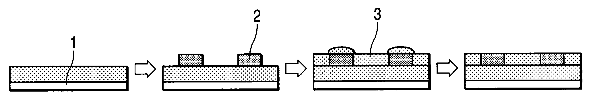
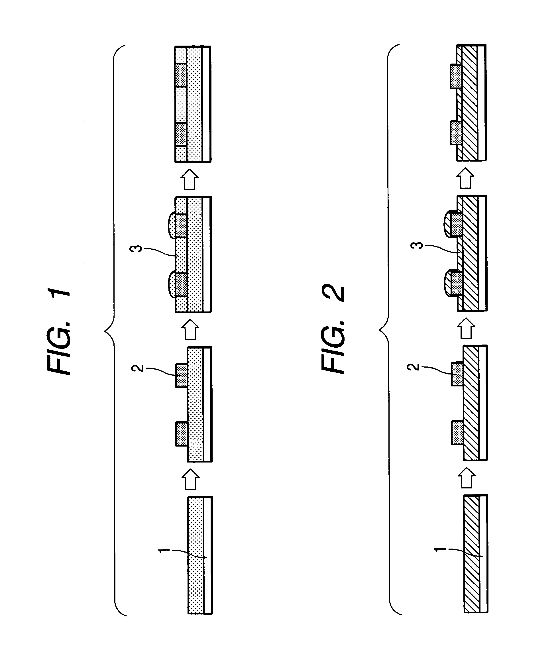
[0041]As shown in FIG. 1, internal electrodes 2 having a predetermined thickness are formed on a substrate 1 by a discretional process. Then slurry of a photosensitive ceramic 3 is applied on the surface of the internal electrodes. The slurry is dried so that the thickness thereof just before exposure will be substantially equal to the thickness of the internal electrodes. Subsequently, the photosensitive ceramic slurry is irradiated with light from the upper side of the substrate to effect exposure while the internal electrode pattern is masked by a photo mask 4 as shown in FIG. 4. In this process, the surface of the photosensitive ceramic slurry is selectively hardened while controlling the exposure amount in such a way that the exposed portion on the surface of the photosensitive ceramic slurry is hardened. The portion of the photosensitive ceramic slurry that has not been exposed is removed by development process to produce a substantially flat layer incorporating internal elect...

embodiment 2

[0045]As shown in FIG. 2, internal electrodes 2 having a predetermined thickness 2 are formed on a substrate 1 by a discretional process. Then slurry of a photosensitive ceramic 3 is applied on the surface of the internal electrodes. The slurry is dried so that the thickness thereof just before exposure will be smaller than the thickness of the internal electrodes. Subsequently, the photosensitive ceramic slurry is irradiated with light from the upper side of the substrate to effect exposure while the internal electrode pattern is masked by a photo mask 4 as shown in FIG. 4. In this process, the surface of the photosensitive ceramic slurry is selectively hardened while controlling the exposure amount in such a way that the exposed portion on the surface of the photosensitive ceramic slurry is hardened. The portion of the photosensitive ceramic slurry that has not been exposed is removed by development process to expose the internal electrode pattern.

[0046]Circuit boards or electroni...

embodiment 3

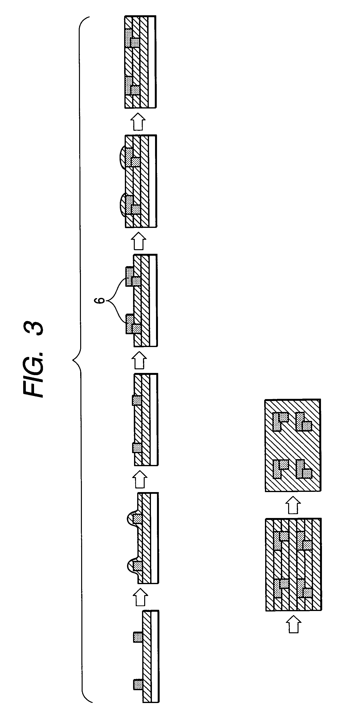
[0047]As shown in FIG. 3, internal electrodes 2 having a predetermined thickness are formed on a substrate 1 by a discretional process. Then slurry of a photosensitive ceramic 3 is applied on the surface of the internal electrodes. The slurry is dried so that the thickness thereof just before exposure will be smaller than the thickness of the internal electrodes. Subsequently, the photosensitive ceramic slurry is irradiated with light from the upper side of the substrate to effect exposure while the internal electrode pattern is masked by a photo mask 4 as shown in FIG. 4. In this process, the surface of the photosensitive ceramic slurry is selectively hardened while controlling the exposure amount in such a way that the exposed portion on the surface of the photosensitive ceramic slurry is hardened. The portion of the photosensitive ceramic slurry that has not been exposed is removed by development process to expose the internal electrode pattern. On the post electrodes thus formed...


PUM

PropertyMeasurementUnit
thicknessaaaaaaaaaa
thicknessaaaaaaaaaa
thicknessaaaaaaaaaa

Abstract

The present invention provides a method for manufacturing an electronic part that can cope with downsizing, improvement in performance and quality of a multilayer electronic part. A ceramic green sheet is produced by forming on a substrate or on a layer formed on a substrate an internal electrode having a predetermined thickness by a discretional process, forming a photosensitive ceramic slurry on a surface of the substrate or the layer and the internal electrode in such a way that its thickness just before exposure will be substantially equal to or smaller than the thickness of the internal electrode from the surface of the substrate or the layer, irradiating the photosensitive ceramic slurry with light from the upper side of the substrate to perform exposure while masking the internal electrode pattern, to selectively harden the surface of the photosensitive ceramic slurry, the exposure amount being controlled in such a way that the surface of the photosensitive ceramic slurry is hardened, and removing the portion of the photosensitive ceramic slurry that has not been exposed by a development process to expose a surface of the internal electrode pattern.

Description

BACKGROUND OF THE INVENTION[0001]1. Field of the Invention[0002]The present invention relates to a method for manufacturing electronic parts, which are exemplified by electronic parts made of so-called multilayer ceramic formed by laminating ceramic green sheets. More particularly, the present invention relates to a method for manufacturing what is called a ceramic green sheet incorporating an electrode layer inside. Examples of the multilayer ceramic electronic parts described herein include multilayer ceramic capacitors, multilayer ceramic inductors, LC composite parts including them and EMC related parts.[0003]2. Related Background Art[0004]In recent years, with downsizing and rapid popularization of electronic apparatuses represented by cellular phones, an increase in mounting density of the electronic parts used for those apparatuses and improvement in their performance, are required. To meet these requirements, demands for downsizing and improvement in functions, which will be...

Claims


Application Information

Patent Timeline
Patent Type & Authority Patents(United States)
IPC IPC(8): B32B37/00B32B38/00H01F41/00H01G13/00H01G4/12C03B29/00H01F17/00H01F41/04H01G4/00H01G4/30H05K1/03H05K1/09H05K3/00H05K3/06H05K3/46
CPCC04B35/6269H01G4/30H05K3/4667H05K1/0306H05K2203/0514H05K2201/09881H05K3/0023H01G4/12H01F17/00H01F41/04
Inventor YOSHIDA, MASAYUKIAOKI, SHUNJISUTOH, JUNICHIWATANABE, GENICHI
Owner TDK CORPARATION
Why Eureka
Try Eureka