Clock generation circuit capable of setting or controlling duty ratio of clock signal and system including clock generation circuit
a technology of clock signal and duty ratio, applied in the direction of generating/distributing signals, pulse techniques, instruments, etc., can solve the problems of increasing noise, abrupt increase of power consumption, and reducing operational efficiency
- Summary
- Abstract
- Description
- Claims
- Application Information
AI Technical Summary
Benefits of technology
Problems solved by technology
Method used
Image
Examples
first embodiment
[0056][First Embodiment]
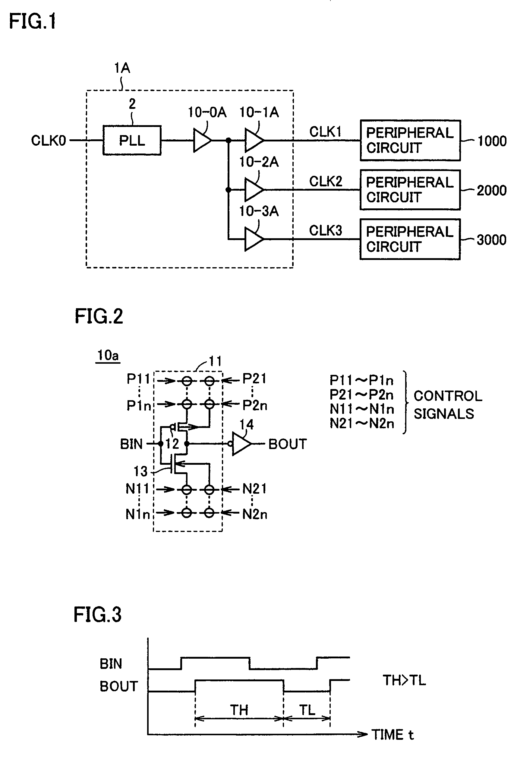
[0057]FIG. 1 is a block diagram showing a clock generation circuit 1A and peripheral circuits thereof in accordance with a first embodiment of the present invention.
[0058]Clock generation circuit 1A of the first embodiment shown in FIG. 1 receives a reference clock signal CLK0 to output clock signals CLK1, CLK2, and CLK3 to peripheral circuits 1000, 2000, and 3000, respectively. Here, peripheral circuits 1000, 2000, and 3000 may be a random logic circuit, an operation circuit, a register circuit, a memory circuit, an analog circuit, or the like.
[0059]Clock generation circuit 1A includes a PLL (Phase Locked Loop) 2, and buffer circuits 10-0A, 10-1A, 10-2A, and 10-3A. PLL circuit 2 receives a reference clock signal CLK0. Buffer circuit 10-0A receives the output from PLL circuit 2. Buffer circuits 10-1A, 10-2A, 10-3A receive the output of buffer circuit 10-0A to output clock signals CLK1, CLK2, CLK3, respectively.
[0060]Clock generation circuit 1A in accordance w...
second embodiment
[0125][Second Embodiment]
[0126]FIG. 14 is a block diagram showing a clock generation circuit 1B and peripheral circuits thereof in accordance with a second embodiment of the present invention.
[0127]Clock generation circuit 1B of the second embodiment shown in FIG. 14 receives reference clock signal CLK0 to output clock signals CLK1, CLK2, CLK3 to peripheral circuits 1000, 2000, 3000, respectively. Here, peripheral circuits 1000, 2000, 3000 may be, for example, a random logic circuit, an operation circuit, a register circuit, a memory circuit, an analog circuit, or the like.
[0128]Clock generation circuit 1B includes a PLL circuit 2B, and buffer circuits 10-0, 10-1, 10-2, 10-3. PLL circuit 2B receives reference clock signal CLK0. Buffer circuit 10-0 receives the output from PLL circuit 2B. Buffer circuits 10-1, 10-2, 10-3 receive the output from buffer circuit 10-0 to output clock signals CLK1, CLK2, CLK3, respectively.
[0129]Clock generation circuit 1B of the second embodiment is conf...
third embodiment
[0160][Third Embodiment]
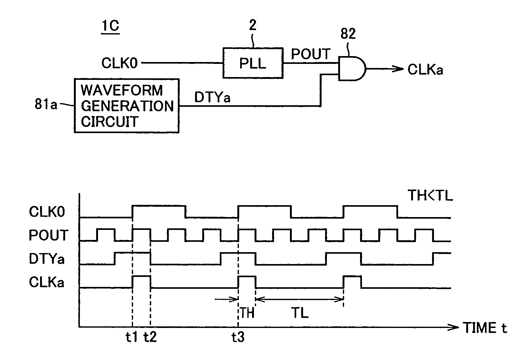
[0161]FIG. 19 is a circuit diagram showing a circuit configuration of a clock generation circuit 1C in accordance with a third embodiment of the present invention.
[0162]Clock generation circuit 1C of the third embodiment shown in FIG. 19 includes a PLL circuit 2, a waveform generation circuit 81a, and an AND gate 82.
[0163]PLL circuit 2 receives the input of reference clock signal CLK0 and outputs output PLL signal POUT that is three times the frequency of reference clock signal CLK0. It is noted that PLL circuit 2 may be an analog PLL circuit, a digital PLL circuit, or any other PLL circuit, and that three times is only an example, and basically, any multiplication rate may be employed. Waveform generation circuit 81a outputs a duty ratio control signal DTYa. AND gate 82 receives the inputs of output PLL signal POUT and duty ratio control signal DTYa to output a clock signal CLKa.
[0164]Duty ratio control signal DTYa is a periodic signal having a waveform gene...
PUM
 Abstract
Description
Claims
Application Information


