Method for determining photoresist thickness and structure formed using determined photoresist thickness

a technology of photoresist and thickness, applied in the field of semiconductor devices, can solve the problems of reducing yield, generating a swing curve that is not accurate, and high cost and time consumption of generating swing curves, and achieve accurate indication of photoresist thickness, accurate determination of minimum photoresist thickness, and small feature size

Active Publication Date: 2007-06-26
INTEGRATED DEVICE TECH INC
View PDF4 Cites 5 Cited by
  • Summary
  • Abstract
  • Description
  • Claims
  • Application Information

AI Technical Summary

Benefits of technology

[0012]The method of the present invention provides for accurately determining the minimum photoresist thickness that can be used to form a structure on a semiconductor substrate. Because the method of the present invention provides a more accurate indication of photoresist thickness than is obtained using prior art methods, structures having smaller feature sizes can be obtained. Also, process latitude with respect to process variations is maximized. This minimizes manufacturing defects resulting from photoresist size variance, giving increased yield and reduced device failure. Moreover, as a single wafer process is used, the method of the present invention results in significant cost savings as compared to prior

Problems solved by technology

The process of generating a swing curve is typically expensive and time consuming due to the number of test wafers that must be fabricated and measured.
Also, random or systematic process variation between wafers

Method used


Image

  • Method for determining photoresist thickness and structure formed using determined photoresist thickness
  • Method for determining photoresist thickness and structure formed using determined photoresist thickness
  • Method for determining photoresist thickness and structure formed using determined photoresist thickness

Examples


Embodiment Construction

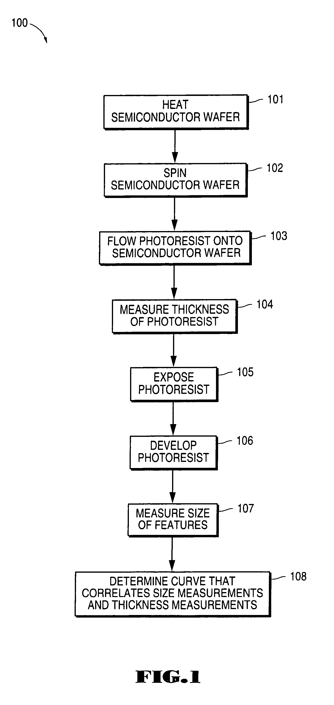
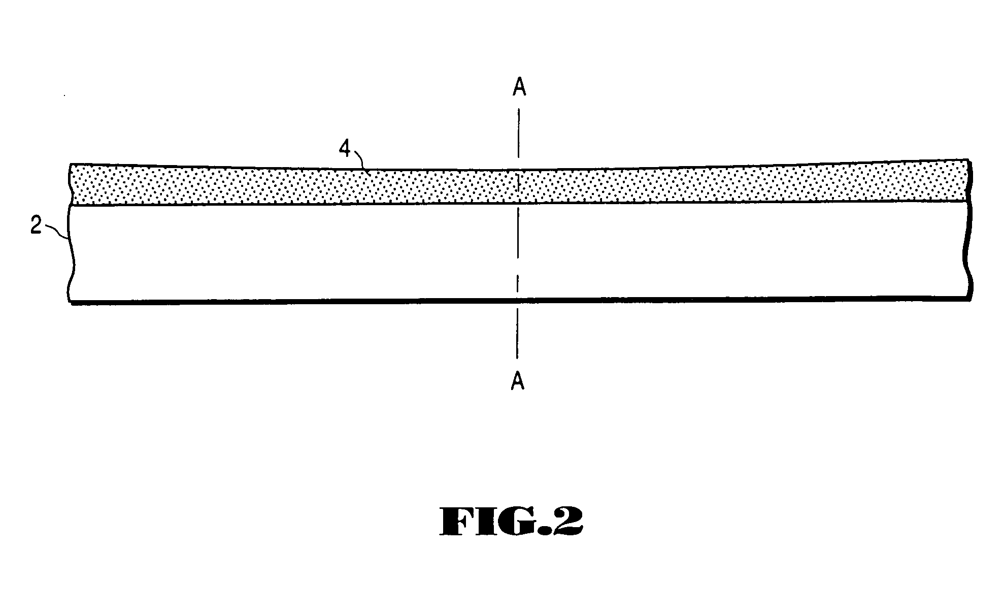
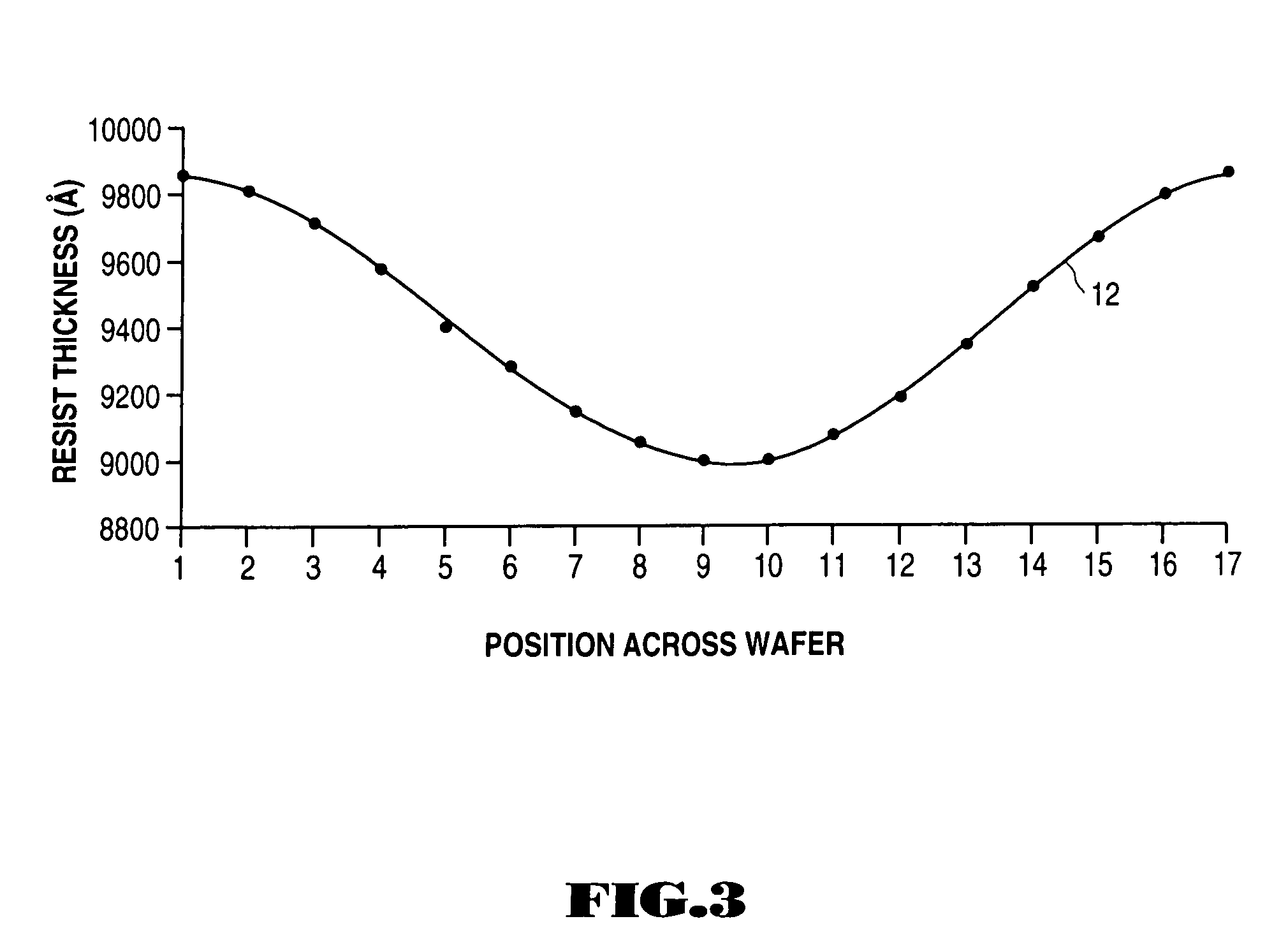
[0034]Reference will now be made in detail to the preferred embodiments of the invention, examples of which are illustrated in the accompanying drawings. While the invention will be described in conjunction with the preferred embodiments, it will be understood that they are not intended to limit the invention to these embodiments. On the contrary, the invention is intended to cover alternatives, modifications and equivalents, which may be included within the spirit and scope of the invention as defined by the appended claims. Furthermore, in the following detailed description of the present invention, numerous specific details are set forth in order to provide a thorough understanding of the present invention. However, it will be obvious to one of ordinary skill in the art that the present invention may be practiced without these specific details. In other instances, well-known methods, procedures, components, and circuits have not been described in detail so as not to unnecessarily...


PUM


Abstract

A method for determining photoresist thickness is disclosed that can be used in a semiconductor fabrication process. A layer of material is formed that has one or more common characteristic relative to the material in the layer that is to be patterned in the semiconductor fabrication process. A layer of photoresist is then formed that has varying thickness. The thickness of the layer of photoresist is determined at a plurality of different points. The layer of photoresist is exposed, developed and etched. The remaining structures are then analyzed to determine photoresist thickness to be used in the semiconductor fabrication process. The determined photoresist thickness is then used in the semiconductor fabrication process to form structures on a semiconductor wafer.

Description

CROSS-REFERENCE TO RELATED APPLICATIONS[0001]This application is a continuation in part of application Ser. No. 10 / 247,877, entitled “METHOD FOR GENERATING A SWING CURVE AND PHOTORESIST FEATURE FORMED USING SWING CURVE,” by Yiming Gu and John L. Sturtevant, filed on Sep. 19, 2002 now U.S. Pat. No. 6,733,936, which is incorporated herein by reference.FIELD OF THE INVENTION[0002]The present invention relates to the field of semiconductor devices. More specifically, the present invention relates to forming photoresist features on a semiconductor wafer.BACKGROUND ART[0003]The size of photoresist features vary with respect to photoresist thickness for a particular wafer substrate. Therefore, it is important to determine a photoresist thickness that will provide the desired photoresist feature size. Conventional processes for determining a thickness that will provide a desired photoresist feature size require the generation of a swing curve.[0004]A swing curve is typically generated by pr...

Claims


Application Information

Patent Timeline
IPC IPC(8): G03C5/00G03F7/16G03F7/30
CPCG03F7/168G03F7/30G03F7/3028
Inventor GU, YIMING
Owner INTEGRATED DEVICE TECH INC
Why Eureka
Try Eureka