Semiconductor device having a layout configuration for minimizing crosstalk

a layout configuration and semiconductor technology, applied in semiconductor devices, digital storage, instruments, etc., can solve the problems of low wiring efficiency, deterioration and malfunction of the memory side, and the control process of arranging wires with equal intervals with respect to complementary bit line pairs based on an automatic wiring scheme is generally impossible, and achieves the effect of reducing crosstalk with bit lines and word lines, and reducing area loss

Active Publication Date: 2007-06-26
SOCIONEXT INC
View PDF3 Cites 6 Cited by
  • Summary
  • Abstract
  • Description
  • Claims
  • Application Information

AI Technical Summary

Benefits of technology

[0007]An objective of the present invention is to provide a semiconductor device in which an overlying signal line can be arranged while crosstalk with bit lines and word lines is decreased and which has a layout structure imposing no restriction on a block arrangement rotation and matching the signal line direction on a chip, such that the area loss due to occurrence of a dead space and / or a change of wire layers is reduced.

Problems solved by technology

Therefore, there is a possibility that crosstalk occurs between these lines and signal lines running between the logic circuits over the memory, and the crosstalk causes characteristic deteriorations and malfunctions on the memory side.
Especially, a control process for arranging wires with equal intervals with respect to complementary bit line pairs based on an automatic wiring scheme has been generally impossible.
Therefore, the wiring efficiency is low.
Furthermore, in both of the above techniques, the running direction of signal lines, which run across an upper layer, with respect to the arrangement direction of the memory block is limited, and a rotation arrangement of memory blocks needs to be carried out according to the direction of metal wires which is determined in an automatic wiring process over a semiconductor device.
Therefore, there is a high possibility that such decreased arrangement flexibility generates a dead space and causes an area loss.
Therefore, an area loss is caused even in this case, and such wiring control requires troublesome efforts, resulting in inefficient production.

Method used


Image

  • Semiconductor device having a layout configuration for minimizing crosstalk
  • Semiconductor device having a layout configuration for minimizing crosstalk
  • Semiconductor device having a layout configuration for minimizing crosstalk

Examples


embodiment 1

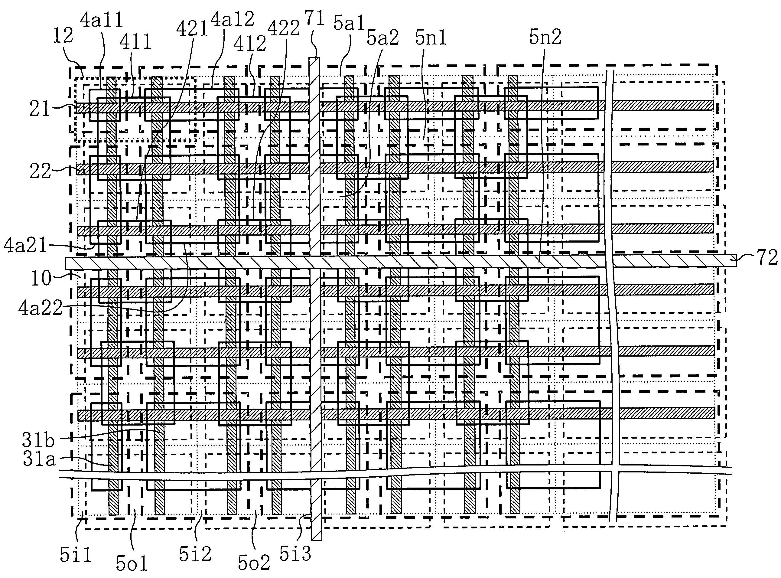
[0020]FIG. 1 shows a layout of a memory cell array portion of a semiconductor device of the present invention. In FIG. 1, reference numeral 10 denotes an entire memory cell array region, which includes a repetition pattern of memory cell units 12 partitioned by cell boundaries 11. Word lines (21, 22, 23, . . . ) run horizontally through the memory cells 12. Complementary bit line pairs (31a, 31b, . . . ) are formed in a wire layer at a lower level than the word lines (21, 22, 23, . . . ) so as to run vertically through the memory cells 12. Over the memory cell array having such a structure, dummy wire patterns (4a1, 4a2, . . . ) are formed such that each dummy wire pattern covers two word lines (for example, the dummy wire pattern 4a1 covers two word lines 21 and 22). Between the dummy wire patterns (4a1, 4a2, . . . ), wire channels (5a1, 5a2, . . . ) of the same metal layer are provided at every other central position between the word lines (21, 22, 23, . . . ).

[0021]Automatic wir...

embodiment 2

[0024]FIG. 3 shows a layout of a memory cell array portion in a semiconductor device of the present invention. In FIG. 3, a memory cell array 10 is divided into two sub-array regions 1a1 and 1a2. In each of the sub-array regions 1a1 and 1a2, dummy wire patterns are provided in a wire layer lying over the word lines (21, 22, 23, . . . ) such that each dummy wire pattern covers four of the bit lines (31a, 31b, 32b, 32a, 33a, 33b, 34b, 34a, . . . ). Herein, dummy wire patterns 4b1, 4b2, . . . are included in the sub-array region 1a1, and dummy wire patterns 4c1, 4c2, 4c3, . . . are included in the sub-array region 1a2. It should be noted, however, that the dummy wire pattern 4c1 of the sub-array region 1a2 is formed to cover only two bit lines, the bit lines 31aand 31b. Accordingly, wire channels (5c, 5c2, . . . ) provided between the dummy wire patterns in the sub-array region 1a2 are shifted horizontally by two bit lines from wire channels (5b1, 5b2, 5b3, . . . ) provided between th...

embodiment 3

[0028]FIG. 4 shows a layout of a type-1 memory cell array portion in the semiconductor device of the present invention. In FIG. 4, reference numeral 14 denotes a row decoder which includes word line drivers, reference numeral 15 denotes a data input / output section which includes sense amplifiers, and reference numeral 16 denotes a control circuit. In the block of FIG. 4, in a layer lying on a wire layer which includes word lines (21, 22, . . . ) over the memory cell array region 10, dummy wire patterns (4d1, 4d2, . . . ) are formed so as to cover every one of bit lines (31a, 31b, . . . ). Between the dummy wire patterns (4d1, 4d2, . . . ) are wire channels (5e1, 5e2, 5e3, . . . ). In another overlying layer lying on the first dummy wire pattern layer, dummy wire patterns (4e1, 4e2, . . . ) are formed so as to cover every one of the word lines (21, 22, . . . ). Between the dummy wire patterns (4e1, 4e2, . . . ) are wire channels (5f1, 5f2, 5f3, . . . ). Since the bit lines (31a, 31b...


PUM


Abstract

Over a memory cell array region of a static RAM (random access memory), dummy wire patterns are formed such that each dummy wire pattern covers 2×2 horizontally and vertically-adjacent intersection points of word lines and bit lines, and horizontally-running wire channels and vertically-running wire channels are formed between the dummy wire patterns in a lattice configuration. Then, a signal line is automatically arranged to extend through any of the wire channels. The dummy wire patterns are provided in a layer lying on the word lines, and the signal line is provided as a metal line extending in the same layer as that of the dummy wire patterns.

Description

BACKGROUND OF THE INVENTION[0001]The present invention relates to a semiconductor device which incorporates a memory cell array, such as a static RAM (random access memory), or the like.[0002]The trend of the semiconductor device industry has been such that, in a semiconductor device wherein a system is implemented on a chip, i.e., a so-called system LSI (large-scale integrated circuit), a large capacity semiconductor memory is incorporated in some cases, and a large number of small-capacity semiconductor memories are incorporated in other cases. In view of the chip layout efficiency, it has been demanded to use an area over a memory block as a wire region for signals transferred between logic circuits incorporated together with the memory block and signals transferred between an IO (input / output) pad and the logic circuits. However, a typical layout of such a semiconductor memory is such that word lines used for selection of a memory cell to be accessed and bit lines used for data ...

Claims


Application Information

Patent Timeline
Patent Type & Authority Patents(United States)
IPC IPC(8): H01L29/00
CPCG11C5/063G11C7/18G11C8/14
Inventor SATOMI, KATSUJI
Owner SOCIONEXT INC
Why Eureka
Try Eureka