Area optimized edge-triggered flip-flop for high-speed memory dominated design

a technology of high-speed memory and flip-flop, which is applied in the direction of pulse generators, pulse techniques, instruments, etc., can solve the problems of limiting the testability of integrated circuit designs with reduced area flip-flops, and achieve the effect of reducing area

Inactive Publication Date: 2007-06-26
MARVELL INT LTD
View PDF6 Cites 32 Cited by
  • Summary
  • Abstract
  • Description
  • Claims
  • Application Information

AI Technical Summary

Problems solved by technology

Other reduced area flip-flops have been proposed, but many of these reduced area flip-flops limit the testability of integrated circuit designs.

Method used


Image

  • Area optimized edge-triggered flip-flop for high-speed memory dominated design
  • Area optimized edge-triggered flip-flop for high-speed memory dominated design
  • Area optimized edge-triggered flip-flop for high-speed memory dominated design

Examples


Embodiment Construction

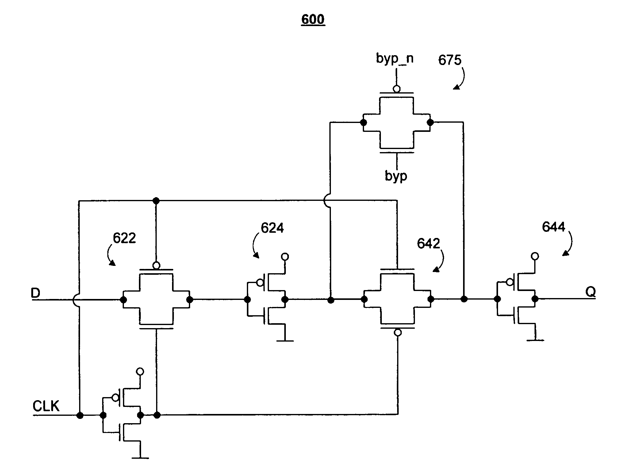
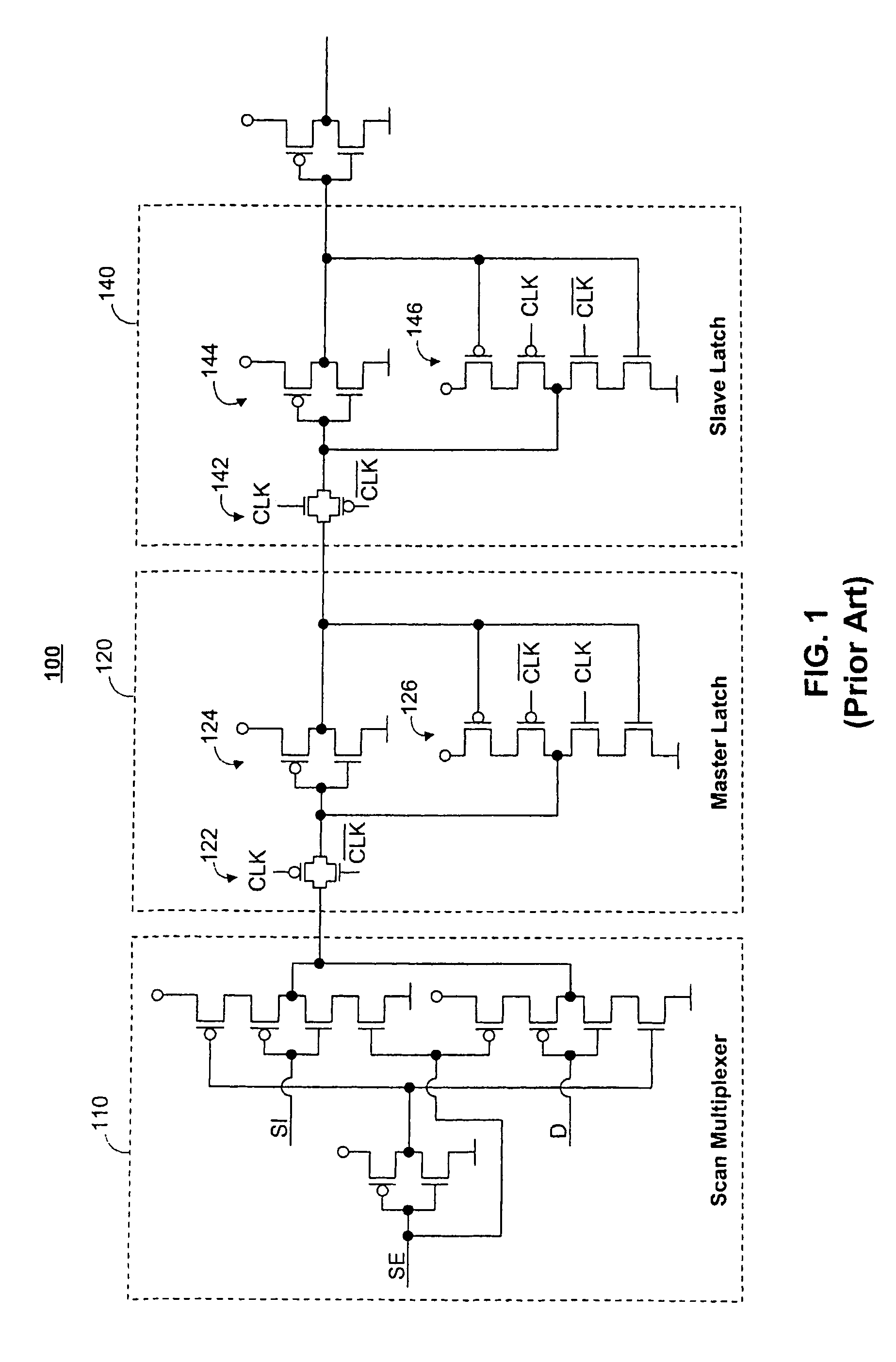
[0017]FIG. 1 shows a simplified schematic of a typical scan flip-flop 100. Scan flip-flop 100 is made up of latch circuits 120 and 140, connected in a master-slave configuration, and multiplexer 110.

[0018]Master latch 120 receives and stores an input signal when the clock signal CLK is at a LOW logic state. While CLK remains at a LOW logic state, passgate 122 is enabled and feedback inverter 126 is disabled, propagating the input of master latch 120 through inverter 124 to the output of master latch 120. When clock signal CLK is at a HIGH logic state, passgate 122 is disabled and feedback inverter 126 is enabled. This cuts-off the input to master latch 120, while preserving the output value of master latch 120.

[0019]Slave latch 140 operates in a similar manner as master latch 120, except with reversed clock inputs. When clock signal CLK is at a HIGH logic state, the input to slave latch 140 is propagated through passgate 142 and inverter 144 to the output of slave latch 140. However...


PUM


Abstract

An area optimized edge-triggered flip-flop for high-speed memory dominated design is provided. The area optimized flip-flop also provides a bypass mode. The bypass mode allows the area optimized flip-flops to act like a buffer. This allows the area optimized flip-flop to provide the basic functionality of a flip-flop during standard operation, but also allows the area optimized flip-flop to act like a buffer when desirable, such as during modes of testing of the design. The area optimized flip-flop provides most of the functionality of a typical flip-flop, while reducing the total area and power consumption of the design.

Description

[0001]This application claims the benefit of provisional application 60 / 563,294 filed Apr. 15, 2004, which is hereby incorporated by reference herein in its entirety.BACKGROUND OF THE INVENTION[0002]This invention relates to high-speed, register dominated integrated circuit designs. More particularly, this invention relates to an area optimized flip-flop for reducing the total area of the integrated circuit design.[0003]In high-speed, register dominated integrated circuit designs, flip-flops make up a significant portion of the total design area. Thus, optimizing or reducing the area of flip-flops in these designs, may significantly improve the designs by reducing their total area and power consumption.[0004]Other reduced area flip-flops have been proposed, but many of these reduced area flip-flops limit the testability of integrated circuit designs. For example, scan chain testing is one commonly used test technique. A group of flip-flops within an integrated circuit design may be ...

Claims


Application Information

Patent Timeline
Patent Type & Authority Patents(United States)
IPC IPC(8): G01R31/28
CPCG11C29/32G11C2029/3202
Inventor KATCHMART, SUPAKET
Owner MARVELL INT LTD
Why Eureka
Try Eureka