Conductor crossover for a semiconductor detector

a semiconductor detector and crossover technology, applied in the direction of instruments, x/gamma/cosmic radiation measurement, radio frequency control devices, etc., can solve the problems of electrical drift field, design of connecting conductors representing general problems, and total depletion of semiconductor substrates

Inactive Publication Date: 2007-07-03
MAX PLANCK GESELLSCHAFT ZUR FOERDERUNG DER WISSENSCHAFTEN EV
View PDF8 Cites 31 Cited by
  • Summary
  • Abstract
  • Description
  • Claims
  • Application Information

AI Technical Summary

Benefits of technology

[0007]An object of the invention is to provide an improved conductor crossover for a semiconductor detector which eliminates the disadvantages of conventional conductor crossovers and which...

Problems solved by technology

The design of the connecting conductor represents a general problem in the production of semiconductors.
In the effective region of the electrodes this results in total depletion of the semiconductor substrate, and also produces an electrical drift field in the semiconductor substrate.
The design of the connecting conductor to the anode has thus far represented a significant problem in the drift detectors.
On account of the large differences in potential between the connecting conductor and the semiconductor substrate together with the semiconductor electrodes, the above-referenced guiding of the connecting conductor over the semiconduct...

Method used


Image

  • Conductor crossover for a semiconductor detector
  • Conductor crossover for a semiconductor detector
  • Conductor crossover for a semiconductor detector

Examples


Embodiment Construction

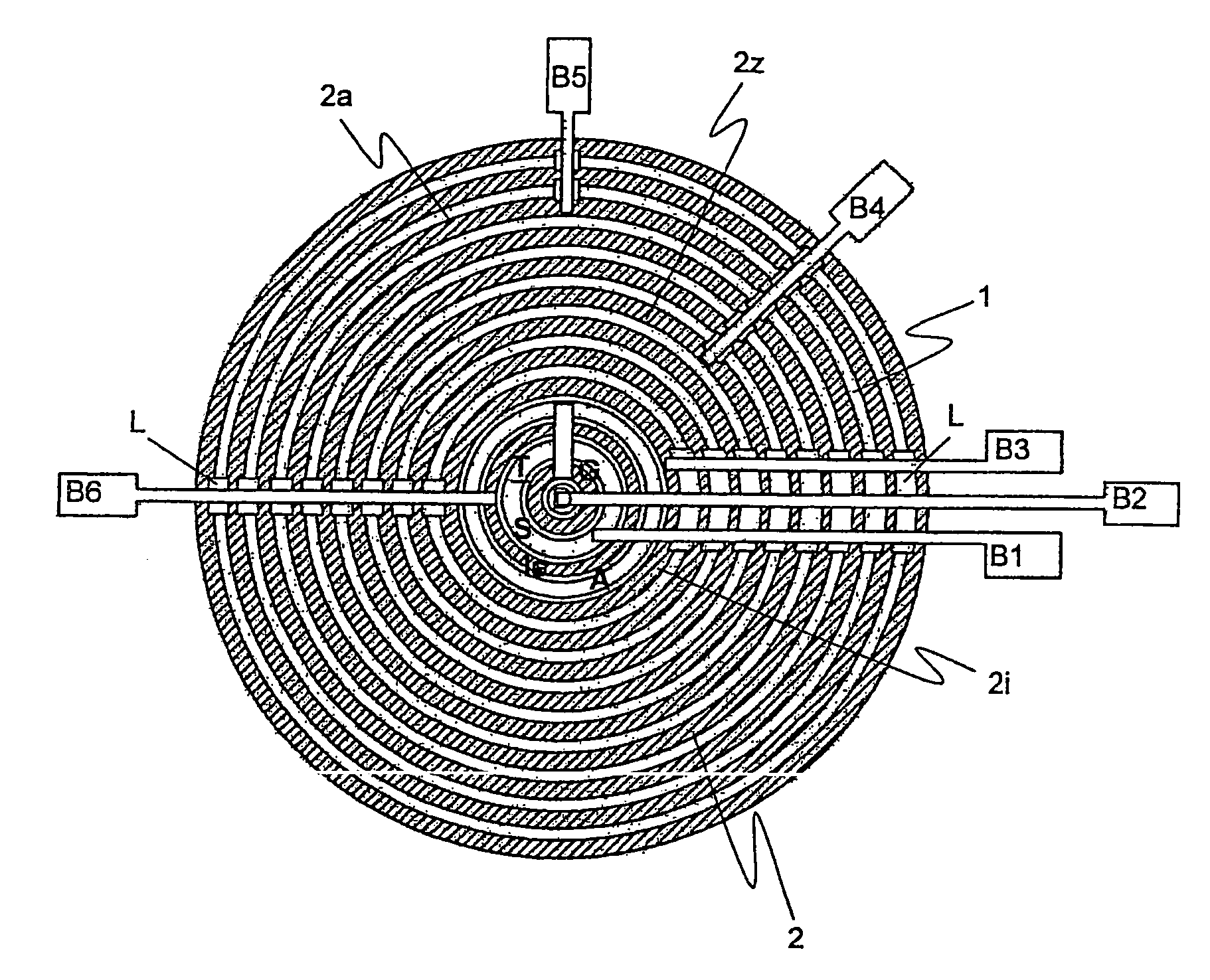
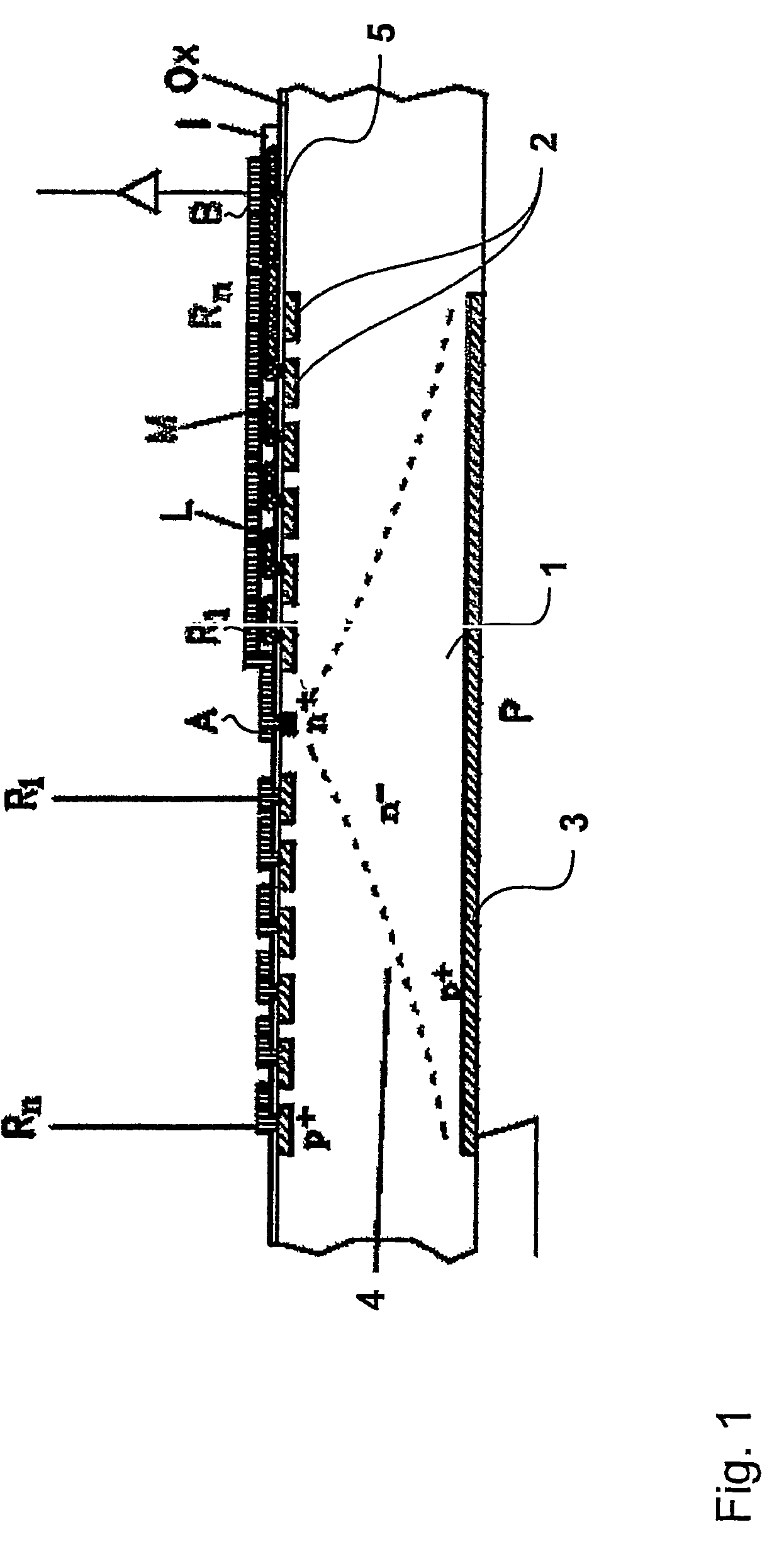
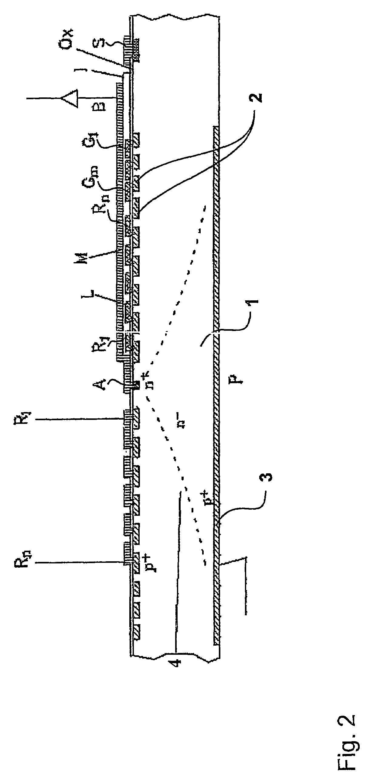
[0028]FIG. 1 shows a silicon drift detector in an enlarged cross-sectional view, which may be used in X-ray spectroscopy, for example. The cylindrical drift detector comprises a semiconductor substrate 1, on the surface of which doped regions form semiconductor electrodes 2, 3, and A. Radiation detection is performed by the detection of electrons which are released by the radiation in the semiconductor substrate 1, the semiconductor electrodes interacting in a manner known as such, as described for example by L. Strüder in the above-referenced publication. The semiconductor substrate 1 comprises an n-doped silicon disk, the doping being so weak that the semiconductor substrate 1 is totally depleted in the sensitive region. The semiconductor substrate 1 has, for example, a thickness of approximately 300 μm and a diameter of several mm, depending on the application, such as approximately 2.5 mm, or up to several cm, for example 10 cm.

[0029]The readout electrode A, which is made out of...


PUM


Abstract

The invention relates to a conductor crossover for a semiconductor detector, particularly for a drift detector for conducting X-ray spectroscopy. The conductor crossover comprises at least two doped semiconductor electrodes (2), which are placed inside a semiconductor substrate (1), at least one connecting conductor (M), which is guided over the semiconductor electrodes (2), and a first insulating layer (Ox). An intermediate electrode (L) is situated between the connecting conductor (M) and the first insulation layer (Ox). Said intermediate electrode overlaps the area of the semiconductor substrate (1) between the semiconductor electrodes (2) and is electrically insulated from the connecting conductor (M) by at least one additional insulation layer (I). The invention also relates to a drift detector equipped with a conductor crossover of this type and to a detector arrangement for conducting X-ray spectroscopy.

Description

CROSS REFERENCE TO RELATED APPLICATIONS[0001]This application is a National Stage application of international application No. PCT / EP03 / 03209 filed on Mar. 27, 2003 in the European Receiving Office, priority from which is here claimed.BACKGROUND OF THE INVENTION[0002]Semiconductor detectors for detecting electromagnetic radiation are based on the measurement of free charge carriers which are generated by the radiation in a semiconductor component. The charge carriers produce an electrical signal, which is conducted over at least one connecting conductor to a measuring device. The design of the connecting conductor represents a general problem in the production of semiconductors. The detector together with the connecting conductor must be practicable to manufacture and easy to handle, but must also not impair the detector function via the connecting conductor.[0003]There are, for example, semiconductor detectors for locally resolved radiation detection which have multiple semiconduct...

Claims


Application Information

Patent Timeline
IPC IPC(8): G01T1/20H01L27/10H01LH01L27/146H01L31/02H01L31/0224H01L31/0352H01L31/115
CPCH01L27/14603H01L31/02002H01L31/022408H01L31/03529H01L31/115Y02E10/50G01T1/2928
Inventor STRUDER, LOTHARLUTZ, GERHARDRICHTER, RAINER
Owner MAX PLANCK GESELLSCHAFT ZUR FOERDERUNG DER WISSENSCHAFTEN EV
Why Eureka
Try Eureka