Integrated circuit device

a technology of integrated circuits and circuits, applied in the direction of superconductor devices, instruments, heat measurement, etc., can solve the problems of lowering the connection reliability, and achieve the effect of high connection reliability, high snr, and high resistivity of metal oxides

Active Publication Date: 2007-07-03
RENESAS ELECTRONICS CORP
View PDF26 Cites 6 Cited by
  • Summary
  • Abstract
  • Description
  • Claims
  • Application Information

AI Technical Summary

Benefits of technology

[0023]According to the invention, the temperature monitor part is connected between the wires through the plugs and the pads. As the resistivity of the metal oxide forming the temperature monitor part changes according to the temperature, the temperature can be measured by measuring the resistance between the wires. As the temperature coefficient of the resistivity of the metal oxide is higher and more stable than the temperature coefficient of the resistivity of the pn junction diode, temperature measurement with a high SNR can be achieved. Because the pads of the aforementioned conductive material are provided between the plugs and the temperature monitor part in the present invention, an insulator film is not formed at the interfaces between the plugs and the temperature monitor part when the temperature monitor part is formed, thus ensuring a high connection reliability between the plugs and the temperature monitor part.
[0024]The metal oxide may be a vanadium oxide (VOx), and the plugs may be formed of tungsten (W). The pads may be formed of one type of a conductive material selected from a group of Ti, TiN, Al, AlCu alloy, Cu, Ta, TaN and NiCr alloy, or a compound of at least two types of conductive materials selected from the group, or a material containing those conductive materials or the compound. When the temperature monitor part of a vanadium oxide is directly formed on the plugs made of tungsten, an insulator film may be formed at the interfaces between the plugs and the temperature monitor part when the temperature monitor part may be formed, lowering the connection reliability. Such formation of an insulator film can be prevented by providing the pads of the aforementioned material between the plugs and the temperature monitor part.
[0025]It is preferable that the integrated circuit device should further include a logic circuit section at least a part of which is laid out directly under the temperature monitor part. This can ensure effective use of a region directly under the temperature monitor part, and thus saves the space required, making it possible to miniaturize an integrated circuit device.
[0027]According to the present invention, the provision of the temperature monitor part of a metal oxide can realize an integrated circuit device with a high-SNR temperature sensor.

Problems solved by technology

When the temperature monitor part of a vanadium oxide is directly formed on the plugs made of tungsten, an insulator film may be formed at the interfaces between the plugs and the temperature monitor part when the temperature monitor part may be formed, lowering the connection reliability.

Method used


Image

  • Integrated circuit device
  • Integrated circuit device
  • Integrated circuit device

Examples


Embodiment Construction

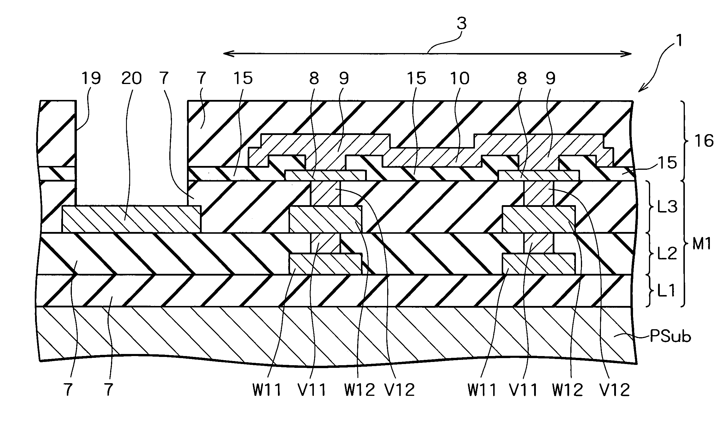
[0033]Preferred embodiments of the present invention will be described specifically below with reference to the accompanying drawings. To begin with, a first embodiment of the present invention will be discussed. FIG. 3 is a cross-sectional view showing a semiconductor integrated circuit device according to the first embodiment of the invention, and FIG. 4 is an equivalent circuit diagram showing the temperature sensor section of the semiconductor integrated circuit device shown in FIG. 3. The semiconductor integrated circuit device according to the present embodiment is formed on a single silicon chip. As shown in FIG. 3, the semiconductor integrated circuit device 1 according to the embodiment is provided with a temperature sensor section 3, a logic circuit section (not shown) and an external pad to connect the internal circuit of the semiconductor integrated circuit device 1 to an external device. The following will describe the structure that is common to the entire semiconducto...


PUM

PropertyMeasurementUnit
thicknessaaaaaaaaaa
thicknessaaaaaaaaaa
thicknessaaaaaaaaaa

Abstract

In a temperature sensor section of a semiconductor integrated circuit device, first vias of tungsten are formed at the topmost layer of a multi-layer wiring layer and pads of titanium are provided on regions of the multi-layer wiring layer which covers the vias. An insulating layer is provided in such a way as to cover the multi-layer wiring layer and the pads, second vias are so formed as to reach the pads. Vanadium oxide is buried in the second vias by reactive sputtering, and a temperature monitor part of vanadium oxide is provided in such a way as to connect the second vias each other. Accordingly, the temperature monitor part is connected between the two wires.

Description

BACKGROUND OF THE INVENTION[0001]1. Field of the Invention[0002]The present invention relates to an integrated circuit device with a built-in monolithic temperature sensor. The present invention can be suitably adapted particularly to a semiconductor integrated circuit device having a temperature sensor fabricated in a semiconductor process.[0003]2. Description of the Related Art[0004]Recently, the need for monitoring the operation temperature of an integrated circuit device is growing for the purpose of preventing thermal breakdown of devices in the integrated circuit device and stabilizing the operation of a device having a temperature-dependent characteristic, such as a crystal oscillator, among those devices which are provided in the integrated circuit device.[0005]In this respect, Japanese Patent Laid-Open Publication No. H1-302849, for example, discloses a technique of protecting an LSI (Large Scale Integrated circuit) in a semiconductor integrated-circuit device from thermall...

Claims


Application Information

Patent Timeline
Patent Type & Authority Patents(United States)
IPC IPC(8): H01L23/58G01K1/14H01L23/48H01L27/06G01K7/00G01K7/01H01L21/4763H01L21/822H01L23/00H01L23/34H01L23/522H01L27/02H01L27/04H01L37/00
CPCG01K7/015H01L23/34H01L23/522H01L27/0248H01L2924/0002H01L2924/00
Inventor OHKUBO, HIROAKIKIKUTA, KUNIKONAKASHIBA, YASUTAKAKAWAHARA, NAOYOSHIMURASE, HIROSHIODA, NAOKISASAKI, TOKUHITOITO, NOBUKAZU
Owner RENESAS ELECTRONICS CORP
Why Eureka
Try Eureka