Scan-path circuit, logic circuit including the same, and method for testing integrated circuit

Inactive Publication Date: 2007-07-03
SHARP KK
View PDF20 Cites 2 Cited by
  • Summary
  • Abstract
  • Description
  • Claims
  • Application Information

AI Technical Summary

Benefits of technology

[0017]The objective of the present invention is to provide a scan-path circuit which make it possible to quickly specify t

Problems solved by technology

Recent upsizing of integrated circuits have made it further difficult to carry out a test for detecting failures in manufactured circuits.
However, the above-described technique has such a problem that, although the presence of a failure on the scan path

Method used


Image

  • Scan-path circuit, logic circuit including the same, and method for testing integrated circuit
  • Scan-path circuit, logic circuit including the same, and method for testing integrated circuit
  • Scan-path circuit, logic circuit including the same, and method for testing integrated circuit

Examples


Embodiment Construction

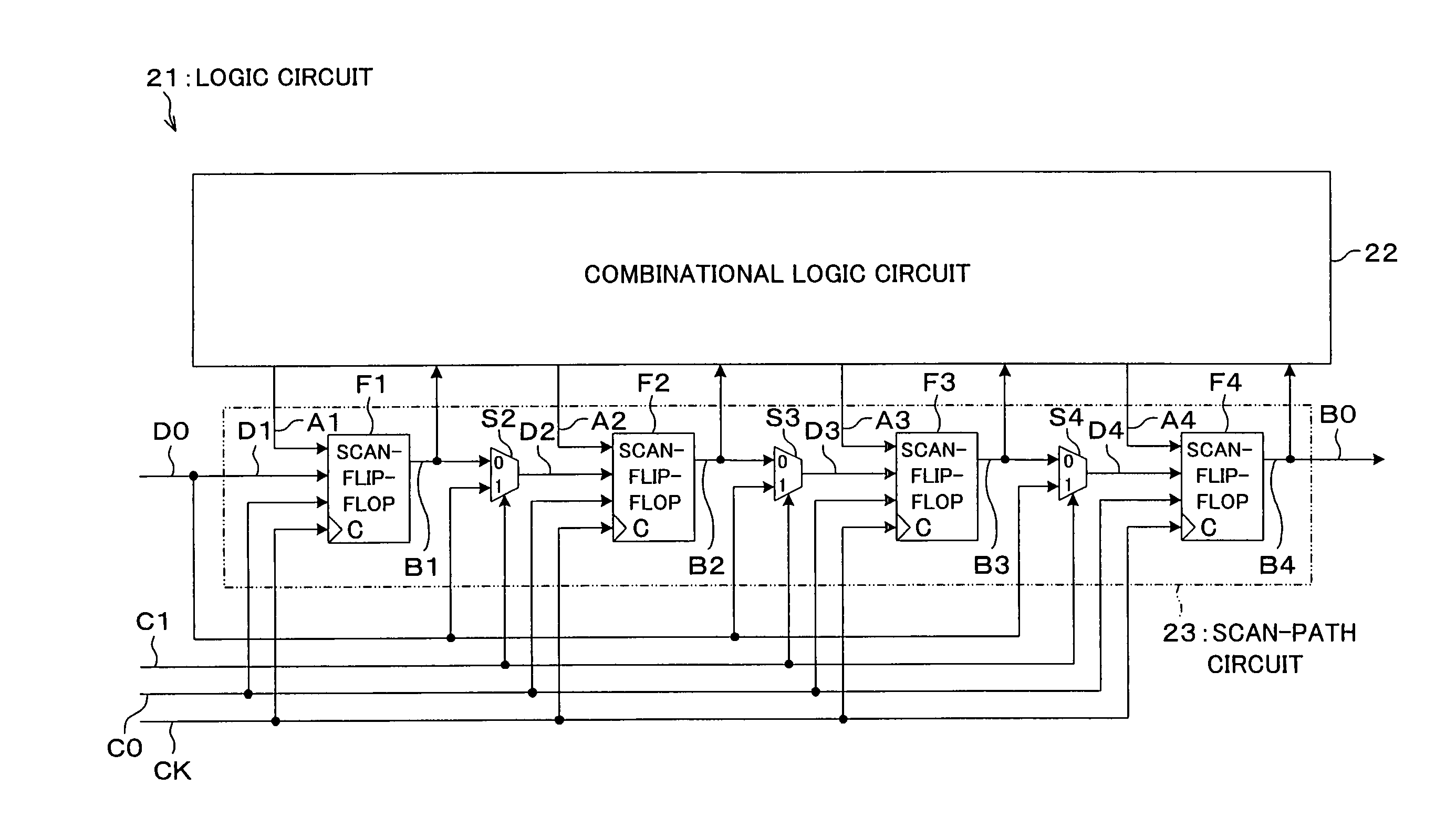
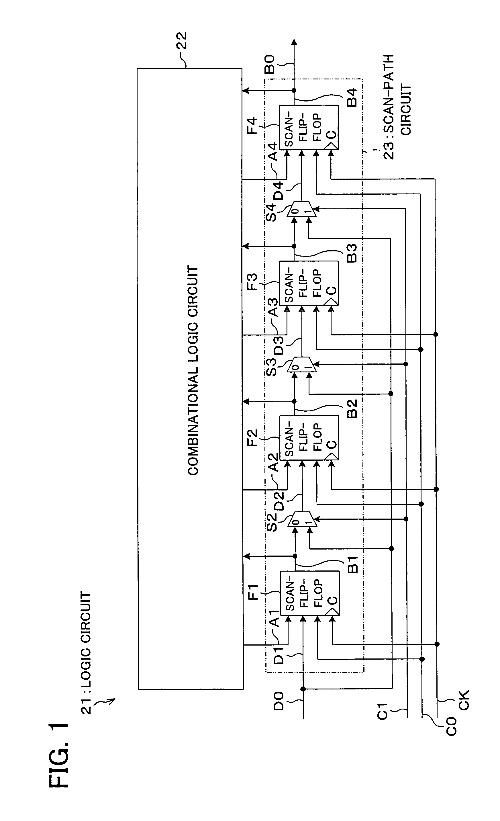
[0027]The following will describe an embodiment of the present invention in reference to FIGS. 1 and 2.

[0028]FIG. 1 is a block diagram showing circuitry of a logic circuit 21 adopting a scan design test technique of the embodiment of the present invention. The logic circuit 21 mainly includes a combinational logic circuit 22 and a scan-path circuit 23. The scan-path circuit 23 is made up of all cascaded flip-flops F1 through Fn (n=4 in FIG. 1) of the logic circuit 21 which is subjected to the test. It should be noted that, on the input sides of the flip-flops F2 through Fn (second and subsequent stages), selectors S2 through Sn are provided, respectively.

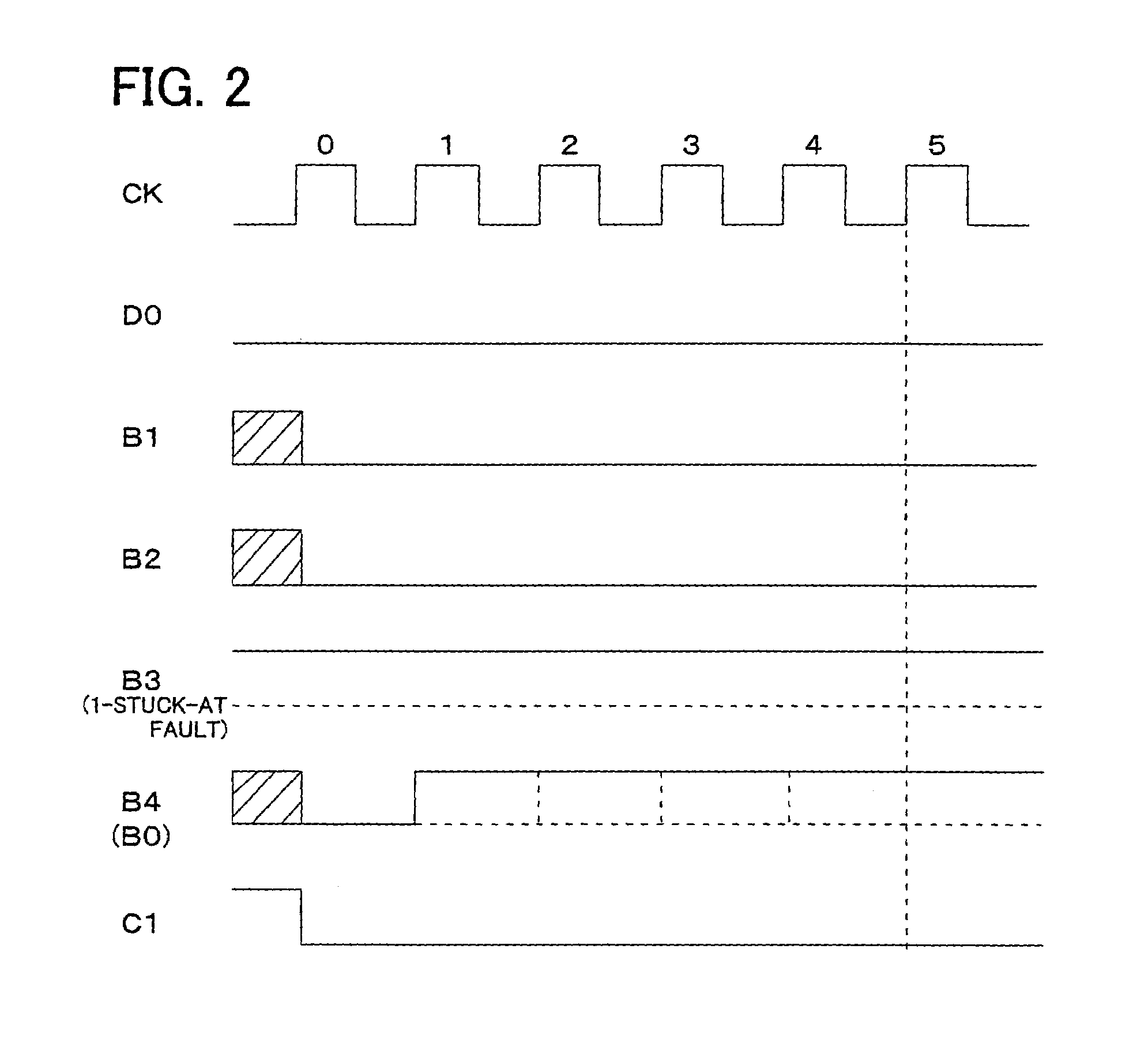
[0029]In normal operation, in response to a clock commonly supplied from the outside to an input terminal CK, the respective flip-flops F1 through Fn fetch signals by respective inputs A1 through An and output the signals from respective outputs B1 through Bn, in repeating fashion. As a result, an arithmetic process is carried out i...


PUM


Abstract

A scan-path circuit is made up of cascaded flip-flops which are input/output circuits of a combinational logic circuit. In a logic circuit 21 which adopts a scan design test technique for simplifying a test of the same by serially shifting a test result through the flip-flops, selectors for directly connecting inputs of the respective flip-flops of the scan-path circuit to a scan input are provided. After causing all flip-flops to have identical values (either “0” or “1”), the values are shifted and outputted so that the location of a failure is specified. With this, the maximum period of time required by the test does not exceed the total of clocks for the shifting through all stages and one more stage. Thus, in addition to the checking of the presence of a failure, the location of a failure is, if necessary, specified in a short period of time.

Description

[0001]This Nonprovisional application claims priority under 35 U.S.C. § 119(a) on Patent Application No. 2003 / 162913 filed in Japan on Jun. 6, 2003, the entire contents of which are hereby incorporated by reference.FIELD OF THE INVENTION[0002]The present invention relates to (i) a scan-path circuit included in a scan-design logic circuit, (ii) the scan-design logic circuit, and (iii) a method for testing an integrated circuit including the logic circuit.BACKGROUND OF THE INVENTION[0003]Recent upsizing of integrated circuits have made it further difficult to carry out a test for detecting failures in manufactured circuits. In order to solve this problem, a scan design (test) technique is adopted for designing circuits. A logic circuit in an integrated circuit is basically made up of a sequential circuit and a combinational circuit. According to the scan design technique, inputs and outputs to / from all flip-flops constituting the sequential circuit are connected to the combinational c...

Claims


Application Information

Patent Timeline
IPC IPC(8): G01R31/28G01R31/3185G06F11/22H01L21/66H01L21/822H01L27/04
CPCG01R31/318544G01R31/318555
Inventor TAKASAKI, TOMOYA
Owner SHARP KK
Why Eureka
Try Eureka