
Method for depositing a film using a charged particle beam, method for performing selective etching using the same, and charged particle beam equipment therefor

a technology of charged particle beam and film, which is applied in the field of method for depositing film using charged particle beam, method for performing selective etching using the same, and charged particle beam equipment therefor, can solve the problems of increasing processing time, small difference in etching rate on the substrate surface within the irradiation region of the fib, and inability to cope with the deposition rate and formation of uniform films

Inactive Publication Date: 2007-07-10
HITACHI HIGH-TECH CORP
View PDF5 Cites 7 Cited by
  • Summary
  • Abstract
  • Description
  • Claims
  • Application Information

AI Technical Summary

Benefits of technology

[0012]Accordingly, one object of the present invention is to provide charged particle equipment capable of forming a film in a desired scanning region more efficiently than the conventional method in the film depositing technology by the use of scanning of a focused charged particle beam, or charged particle equipment capable of selective etching in a desired scanning region more efficiently than the conventional method in the selective etching technology by the use of scanning of a focused charged particle beam.
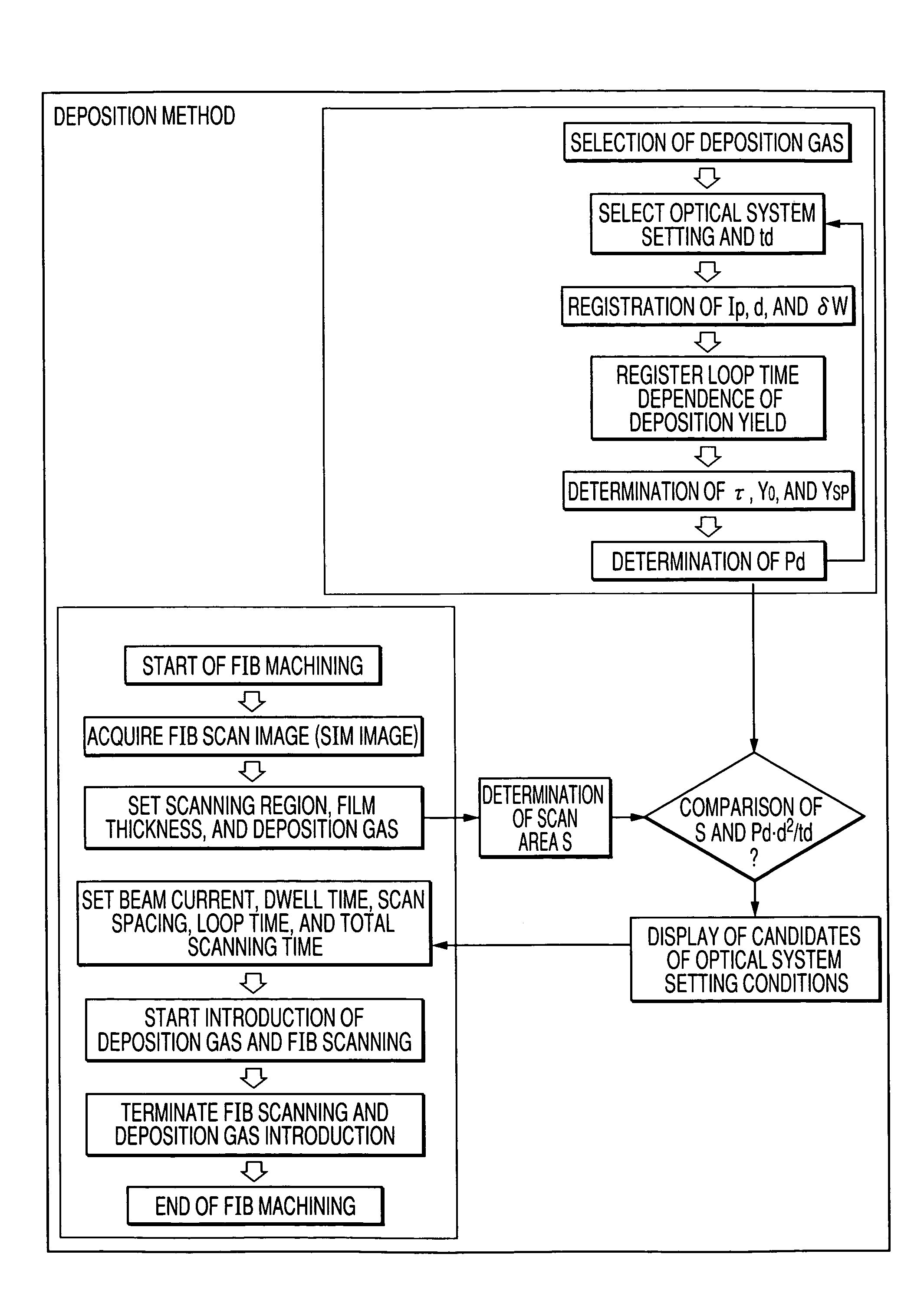
[0015]This invention solves the above-mentioned problem by optimizing processing parameters of each FIB in light of the loop time dependence of the processing speed. By depositing a film according to the scanning method and an irradiation density both of which are based on the above-mentioned setup, a desired film can be formed at high speed, and at the same time the operator can alter the deposition setting in conformity to a desired film quality by reference to display of a judgment result. Consequently, this method can provide a technology of forming a film efficiently in the film-deposition technology by means of scanning of a charged particle beam.

Problems solved by technology

Unfortunately, if the setup by the operator is improper, a film is not formed on the substrate surface at the time of film deposition, and the etching rate difference on the substrate surface within the irradiation region of the FIB is small at the time of selective etching.
However, mere change in the quantity of FIB irradiation cannot lead to equalization of the deposited film, and consequently the technology is not able to cope with the deposition rate and the formation of a uniform film simultaneously.
However, it does not indicate at all how the optical system setting should be optimized for a desired scanning region.
However, since movement of the beam spot is delayed until an etching gas is supplied, the processing time is increased after all.
However, mere change in the quantity of FIB irradiation according to area, position, and shape is insufficient to improve the processing speed.

Method used


Image

  • Method for depositing a film using a charged particle beam, method for performing selective etching using the same, and charged particle beam equipment therefor
  • Method for depositing a film using a charged particle beam, method for performing selective etching using the same, and charged particle beam equipment therefor
  • Method for depositing a film using a charged particle beam, method for performing selective etching using the same, and charged particle beam equipment therefor

Examples


first embodiment

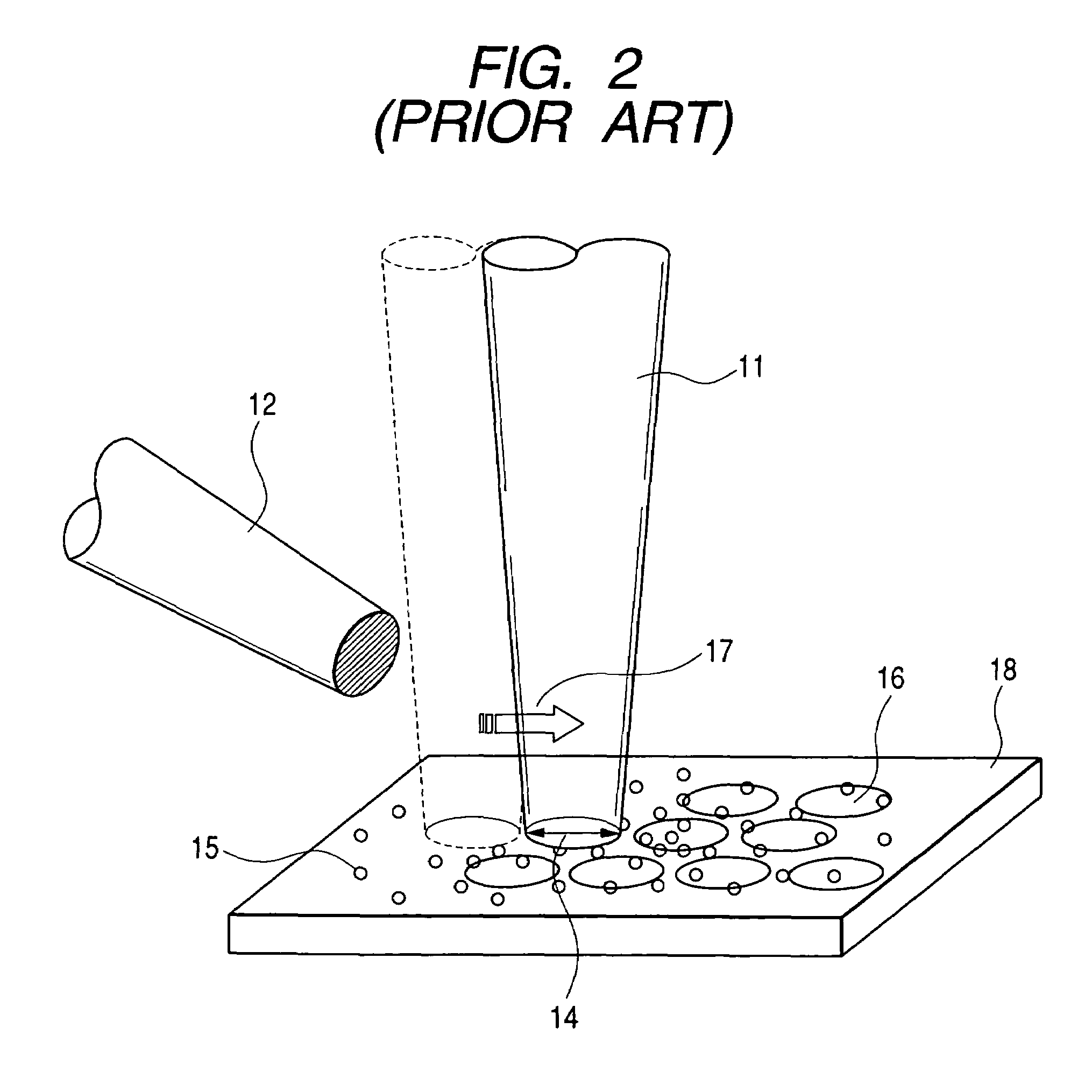
[0055]FIG. 3 shows schematically how a beam spot of a charged particle beam moves in the scanning region, in accordance with an embodiment of the present invention. One circle corresponds to one beam spot, and the beam spot is scanned along the direction of the arrow. Here, the “beam spot” means the size of an area in the sample surface that is occupied by the charged particle beam incident thereon. The center of the beam spot is called a “scan lattice point,” and is designated by the numeral 16 in FIG. 3. The numeral 18 denotes a scanning region, and FIG. 3 shows an example in which the scan lattice points are arranged to form triangular lattices in the scanning region.

[0056]FIG. 4 shows the scan spacing dependence of the deposition rate, in accordance with an embodiment of the present invention. Here, the “scan spacing” means a distance between a certain scan lattice point and a scan lattice point most adjacent to the scan lattice point, and the “deposition rate” is the growth rat...

second embodiment

[0075]In the first embodiment, the optimal values of the deposition parameters, Pd, Td, and d, were found by using the parameters decided from the fitting curves shown in FIGS. 7 through 9. The fitting curves shown in FIGS. 7 though 9 are curves that can be used for years fundamentally once they have been decided. However, there is a case where the fitting curve itself needs to be calibrated due to individual difference of equipment at the time of shipping, variation in deposition conditions, etc. Accordingly, in this embodiment, the fitting curves and a method for calibrating deposition parameters decided by the said curve will be described.

[0076]FIG. 13 shows the deposition-rate calibration screen that is displayed on a user interface screen of the control unit 10 included in the deposition equipment, in accordance with an embodiment of the present invention. The process and material 37 and the beam current 39 can be selected, individually. Here, the process means the kind of proc...

third embodiment

[0082]When a film is deposited by the FIB, there may be a case where a hollow is formed underneath a region where deposition is performed. This hollow is not a cavity in which nothing exists. Rather, the hollow formed is embedded with either a material whose material composition is the same as a film to be deposited or a reaction product of a material of the film to be deposited and a material forming the processed region. The reason for this embedded hollow is because the processed region is partly removed by a sputtering effect before the film is accumulated by the FIB and then the film is accumulated on it.

[0083]FIG. 18 shows how this process proceeds with a diagram showing the cross section of a deposition film, in accordance with an embodiment of the present invention. At a junction plane between the substrate 8 and the deposition film 13, a hollow is formed on the substrate surface by the FIB. When film deposition is done with Ga ions of 30 keV, the sputter depth between film ...


PUM

PropertyMeasurementUnit
sizeaaaaaaaaaa
beam currentaaaaaaaaaa
tilt angleaaaaaaaaaa

Abstract

Certain film deposition and selective etching technology may involve scanning of a charged particle beam along with a deposition gas and etching gas, respectively. In conventional methods, unfortunately, the deposition rate or the selective ratio is oftentimes decreased depending on optical system setting, scan spacing, dwell time, loop time, substrate, etc. Accordingly, an apparatus is provided for finding an optical system setting, a dwell time, and a scan spacing. These parameters are found to realize the optimal scanning method of the charged particle beam from the loop time dependence of the deposition rate or etching rate. This deposition rate or etching rate are measurements stored in advance for a desired irradiation region where film deposition or selective etching should be performed. The apparatus displays a result of its judgment on a display device.

Description

CLAIM OF PRIORITY[0001]The present invention claims priority from Japanese application JP 2003-336691 filed on Sep. 29, 2003, the content of which is hereby incorporated by reference in its entirety.BACKGROUND OF THE INVENTION[0002]1. Field of the Invention[0003]This invention relates to a method for depositing a film by using a deposition gas, a method of selective etching by using an etching gas, charged particle beam equipment for these methods, a method for manufacturing a large scale integration (LSI), and a technology of LSI manufacturing equipment. More particularly, the present invention relates to technology that is effective when being applied to a method for depositing a film by using a deposition gas and a focused ion beam (FIB) or a method for performing selective etching by using an etching gas and a FIB.[0004]2. Discussion of Background[0005]A conventional FIB apparatus can scan the surface of a sample with the FIB, detect secondary electrons and secondary ions genera...

Claims


Application Information

Patent Timeline
Patent Type & Authority Patents(United States)
IPC IPC(8): H01J37/305C23C14/32C23C16/00C23C16/04C23C16/52H01J37/30H01J37/302H01J37/317H01L21/302
CPCC23C16/047C23C16/52H01J37/3023H01J2237/30472H01J2237/31732H01J2237/31745
Inventor FUKUDA, MUNEYUKISHICHI, HIROYASU
Owner HITACHI HIGH-TECH CORP
Learn More