Film forming method and producing method for electron source substrate
a technology of film forming and electron source substrate, which is applied in the manufacture of electrode systems, cold cathode manufacturing, and discharge tube/lamp manufacturing, etc., can solve the problem of inability to avoid a loss in production yield, and achieve the effect of precisely and efficiently forming films and correcting aberrations in the application position of liquid droplets
- Summary
- Abstract
- Description
- Claims
- Application Information
AI Technical Summary
Benefits of technology
Problems solved by technology
Method used
Image
Examples
example 1
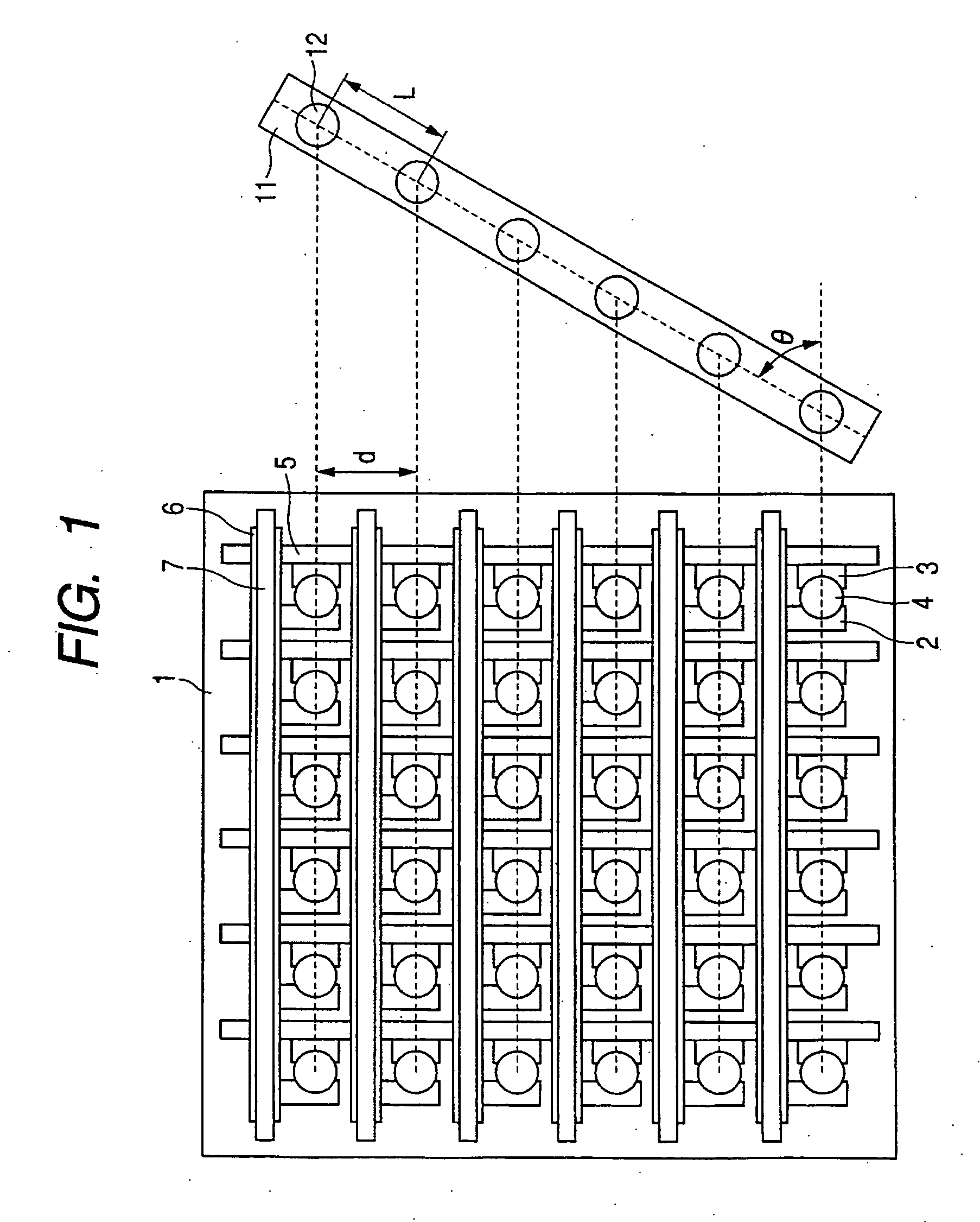
[0050] An electron source substrate was prepared according to a process shown in FIGS. 4 to 9.
[0051] There was employed a substrate 1, prepared by coating and sintering an SiO2 film of a thickness of 100 nm as a sodium blocking layer on a glass PD-200 (manufactured by Asahi Glass Co.) of a thickness of 2.8 mm. It was sufficiently washed with an organic solvent and dried at 120° C.
[0052] Then, on the substrate 1, a Ti film of a thickness of 5 nm as an undercoat layer and a Pt film of a thickness of 40 nm thereon were formed by a sputtering method. Then device electrodes 2, 3 were prepared by patterning these films by a lithographic process of coating, exposure and development of a photoresist followed by etching (FIG. 4). Then an Ag paste was screen printed on the substrate to form lower wirings 5 (FIG. 5). The device electrodes 2, 3 were prepared with a gap of 20 μm, an electrode width of 50 μm, a thickness of 50 nm and a pitch of 1 mm, and the lower wiring 5 was formed with a wid...
example 2
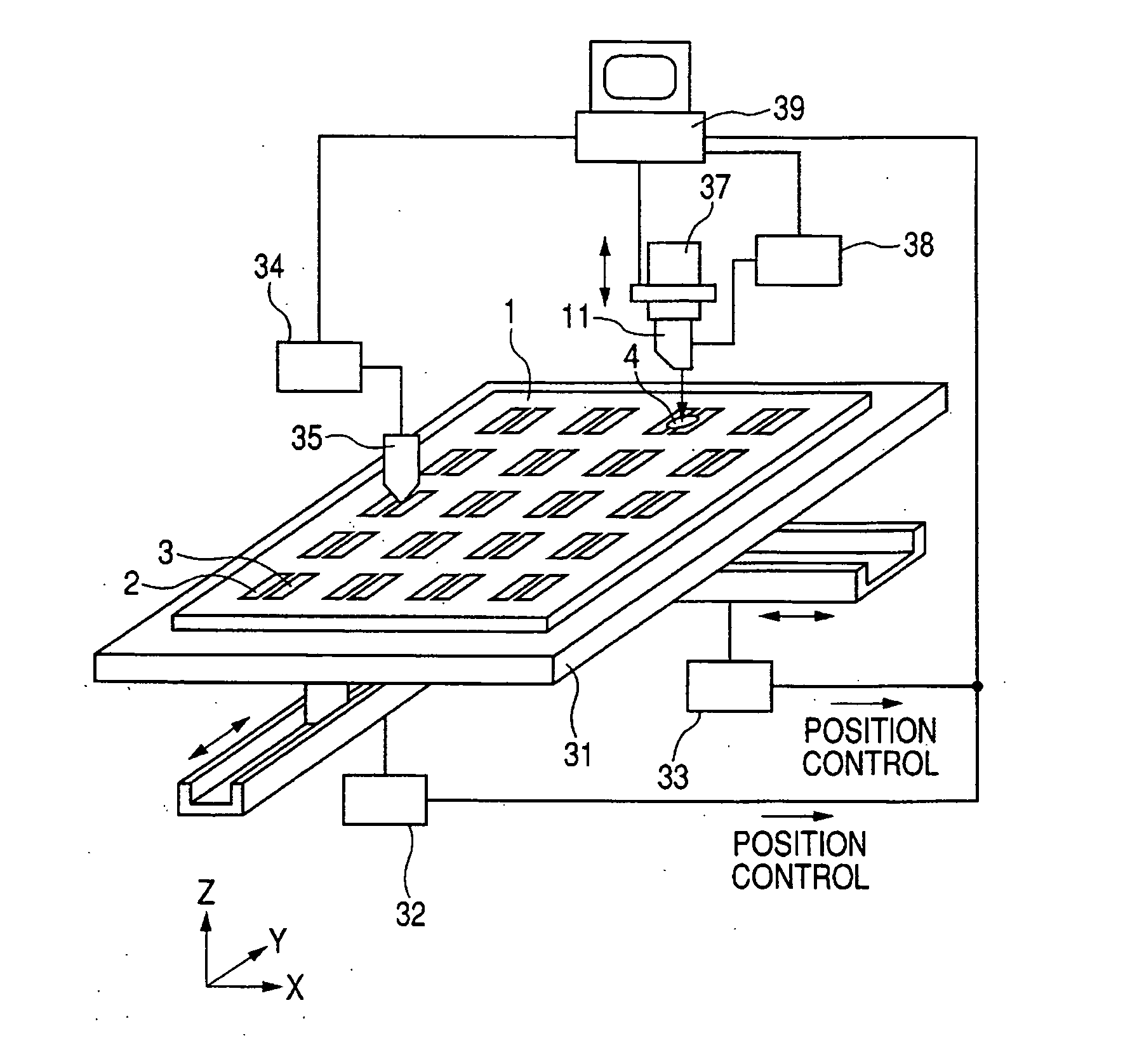
[0059] A process same as in Example 1 was executed up to the preparation of the upper wirings 7. An aqueous solution containing a palladium acetate-ethanolamine complex by 0.2%, isopropyl alcohol by 15%, ethylene glycol by 1% and polyvinyl alcohol by 0.05% was prepared and liquid droplets of such aqueous solution were applied onto the substrate by an equipment as shown in FIG. 3.
[0060] In the present example, the liquid droplet applying step for the above-mentioned aqueous solution was conducted in the following manner:
[0061] [1] An image of individual device area on the substrate 1 was fetched by the CCD camera 35, and the image processing equipment 34 executed a process of extracting an image of the device electrodes 2, 3 from thus fetched image. In the present example, the image extraction was conducted by binarizing the fetched image;
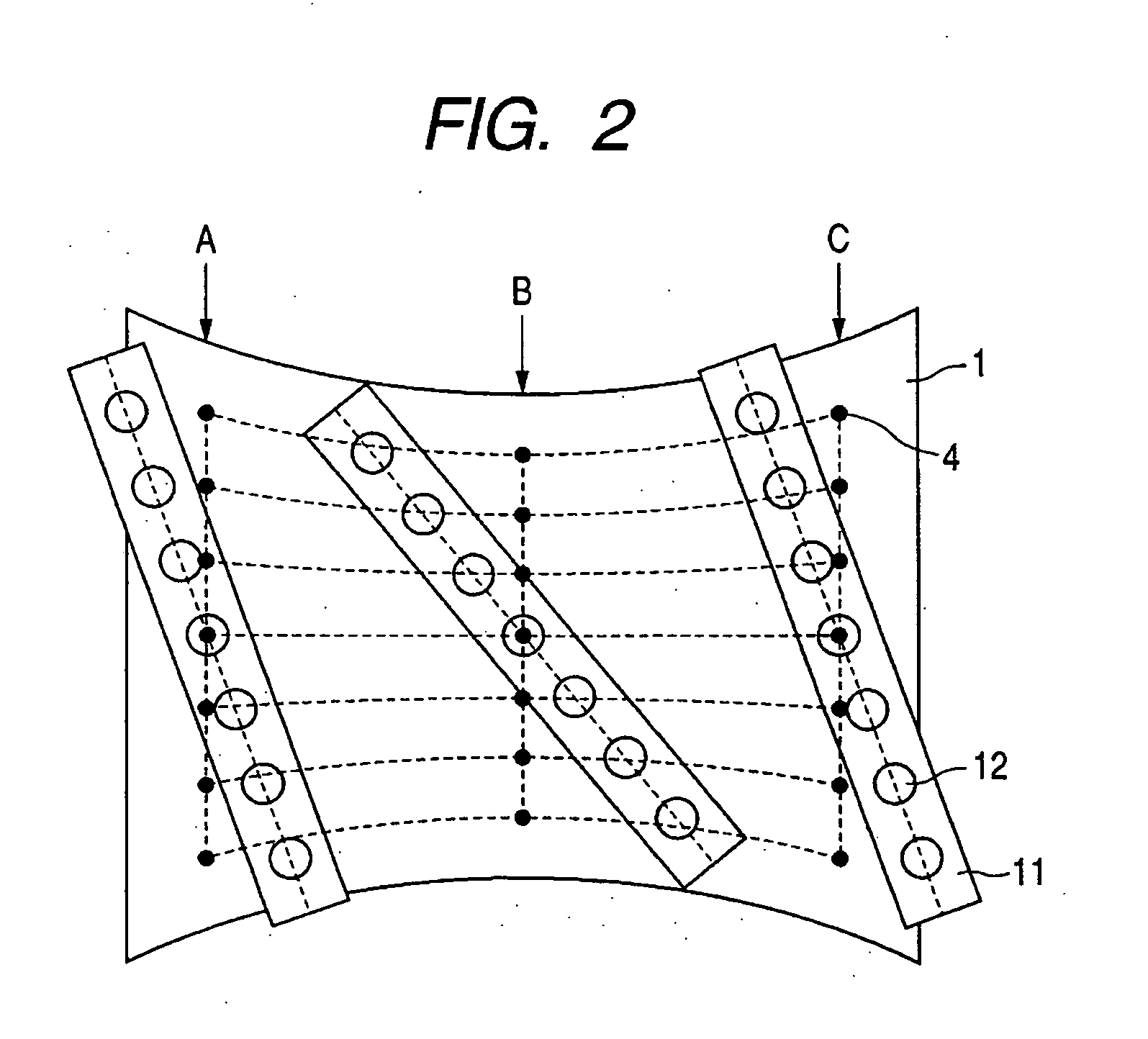
[0062] [2] A liquid droplet applying position (measured value) was calculated by the controlling computer 39, based on the position of center of...
PUM
| Property | Measurement | Unit |
|---|---|---|
| thickness | aaaaa | aaaaa |
| thickness | aaaaa | aaaaa |
| thickness | aaaaa | aaaaa |
Abstract
Description
Claims
Application Information


