Optical waveguide, illumination device, electro-optical device, and electronic apparatus

a technology of illumination device and optical waveguide, which is applied in the direction of lighting and heating apparatus, instruments, and high-level techniques, can solve the problems of insufficient light diffusibility of light generated in a region near point light sources such as leds, and increase consumption of power, so as to suppress the influence of so-called ‘light irregularities', bright illumination, and low power consumption

Active Publication Date: 2007-07-17
BOE TECH GRP CO LTD
View PDF11 Cites 16 Cited by
  • Summary
  • Abstract
  • Description
  • Claims
  • Application Information

AI Technical Summary

Benefits of technology

[0009]An advantage of the invention is that it provides an illumination device in which a region of an optical waveguide is divided into regions and light is emitted from each of the divided regions for partially illuminating a liquid crystal panel, thereby achieving low power consumption.
[0010]According to a first aspect of the invention, an illumination device includes an optical waveguide that has light incident end faces formed at both ends thereof; and light sources that are disposed on the light incident end faces formed at both ends of the optical waveguide. A reflective surface of the optical waveguide has first and second reflective surfaces intersecting at a predetermined boundary line and a light-emitting surface of the optical waveguide has first and second boundary regions divided by the predetermined boundary line. When the light sources provided at one end of the optical waveguide are turned on, light is emitted such that one region of the first and second regions is brighter than the other.
[0011]The illumination device can be used, for example, for a backlight of a liquid crystal display device and includes the optical waveguide that has the light incident end face formed at both ends thereof and the light sources that are disposed on the light incident end faces at both ends of the optical waveguide. Here, for the light source, for example, LEDs are used. The optical waveguide is divided into two regions by the predetermined boundary line, and the reflective surfaces of the respective regions become first and second reflective surfaces. The first and second reflective surfaces cross each other at the predetermined boundary line. According to this aspect, when the light sources provided at one end of the optical waveguide are turned on, light can be emitted such that one of the first and second regions is brighter than the other. In addition, the phrase ‘the light sources disposed on the light incident end faces formed at both ends of the optical waveguide’ includes the case in which the light sources are disposed at any locations of the light incident end faces. That is, it includes the case in which the light sources are disposed at the ends of the light incident end faces, that is, corners of the sides of the optical waveguide, in addition to the case in which the light sources are disposed near the center in a longitudinal direction of the light incident end face.
[0012]Preferably, the first reflective surface reflects the light emitted from the light source disposed on the light incident end face away from the first reflective surface and allows the light to be emitted from the first region, and the second reflective surface reflects the light emitted from the light source disposed on the light incident end face away from the second reflective surface and allows the light to be emitted from the second region. Therefore, when the light sources at one side are turned on, light can be emitted from one of the two regions divided by the boundary line.
[0013]Preferably, the optical waveguide has a cross-section in which a distance between the light-emitting surface and the reflective surface gradually decreases from the predetermined boundary line toward the light incident end faces of both ends. As such, the light incident on one light incident end face is totally reflected with respect to the light-emitting surface in the region of the optical waveguide having the light incident end face, passes through the predetermined boundary line, and is emitted from the light-emitting surface to the exterior in the region of the optical waveguide. Therefore, when the light is incident on the optical waveguide through one light incident end face, only the light-emitting surface in the region opposite to the region having the light incident end face can be brightly illuminated. In addition, by using illumination device having such an optical waveguide, it is possible to suppress the influence of so-called ‘light irregularity’ that diffusibility of the light generated in a region near point light sources such as the LEDs is not sufficient to become dark between light components. In addition, it is possible to increase a light-emitting area of the light-emitting surface.
[0014]Preferably, at least one of the first and second reflective surfaces has a predetermined pattern. According to this aspect, at least one of the first and second reflective surfaces has an angle pattern. An inclined surface of one angle pattern serves to decrease an angle of the light incident on the reflective surface with respect to the light from one of two light incident end faces, and serves to increase an angle of the light incident on the reflective surface with respect to the light from the other of two light incident end faces. Therefore, since the light incident on one light incident end face does not exceed a critical angle with the light-emitting surface, the light is totally reflected at all times. In addition, since the light incident on the other light incident end face exceeds the critical angle with any light-emitting surface, the light is emitted to the exterior from the light-emitting surface. Therefore, it is possible to allow the optical waveguide to partially emit the light by performing the on / off control of the light sources disposed at both ends of the optical waveguide.

Problems solved by technology

For this reason, even though the simple display information can be confirmed, it is necessary that the entire liquid crystal display panel be illuminated whenever the display information is confirmed, which results in an increase in consumed power.
In addition, by using illumination device having such an optical waveguide, it is possible to suppress the influence of so-called ‘light irregularity’ that diffusibility of the light generated in a region near point light sources such as the LEDs is not sufficient to become dark between light components.

Method used


Image

  • Optical waveguide, illumination device, electro-optical device, and electronic apparatus
  • Optical waveguide, illumination device, electro-optical device, and electronic apparatus
  • Optical waveguide, illumination device, electro-optical device, and electronic apparatus

Examples


first embodiment

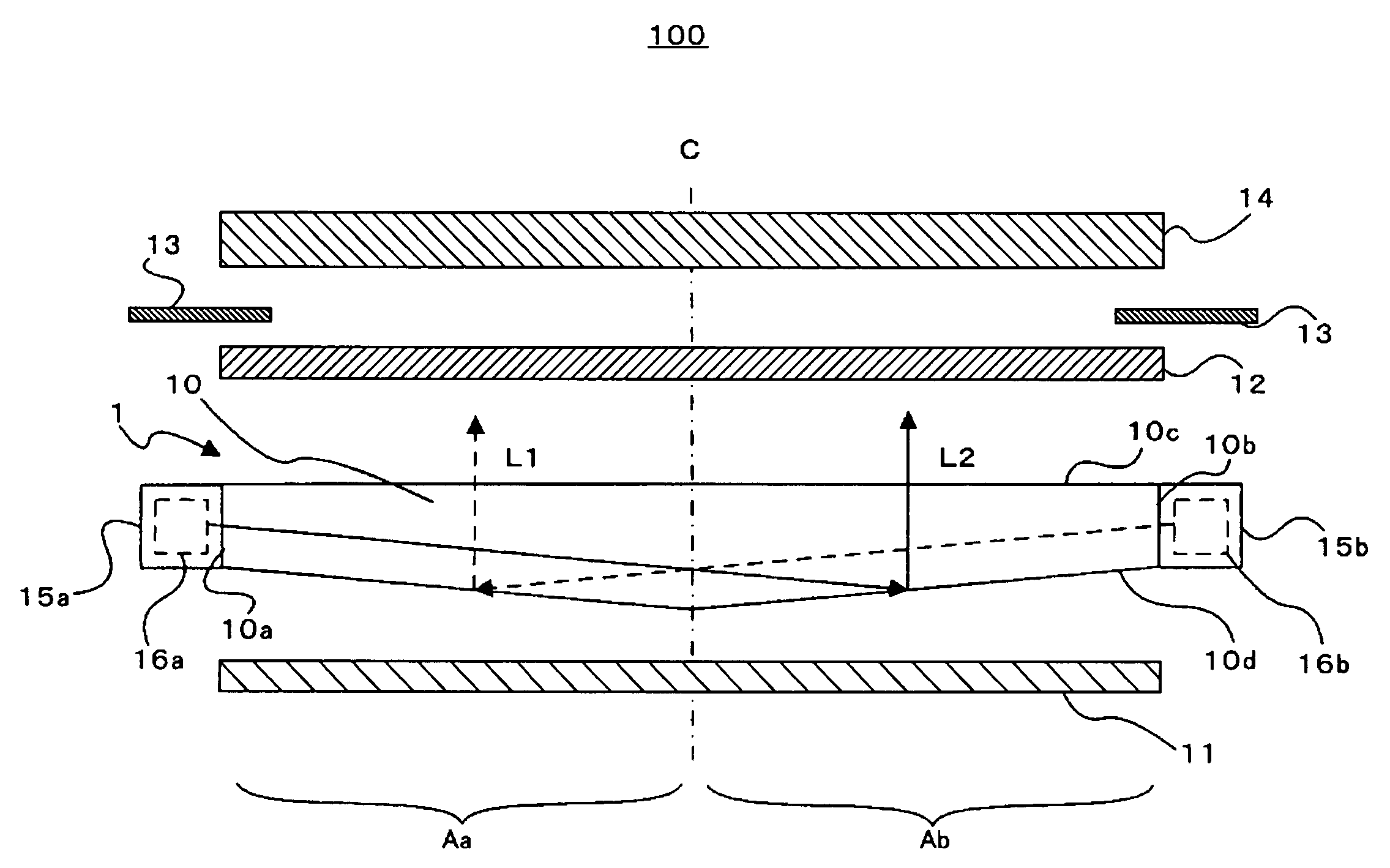
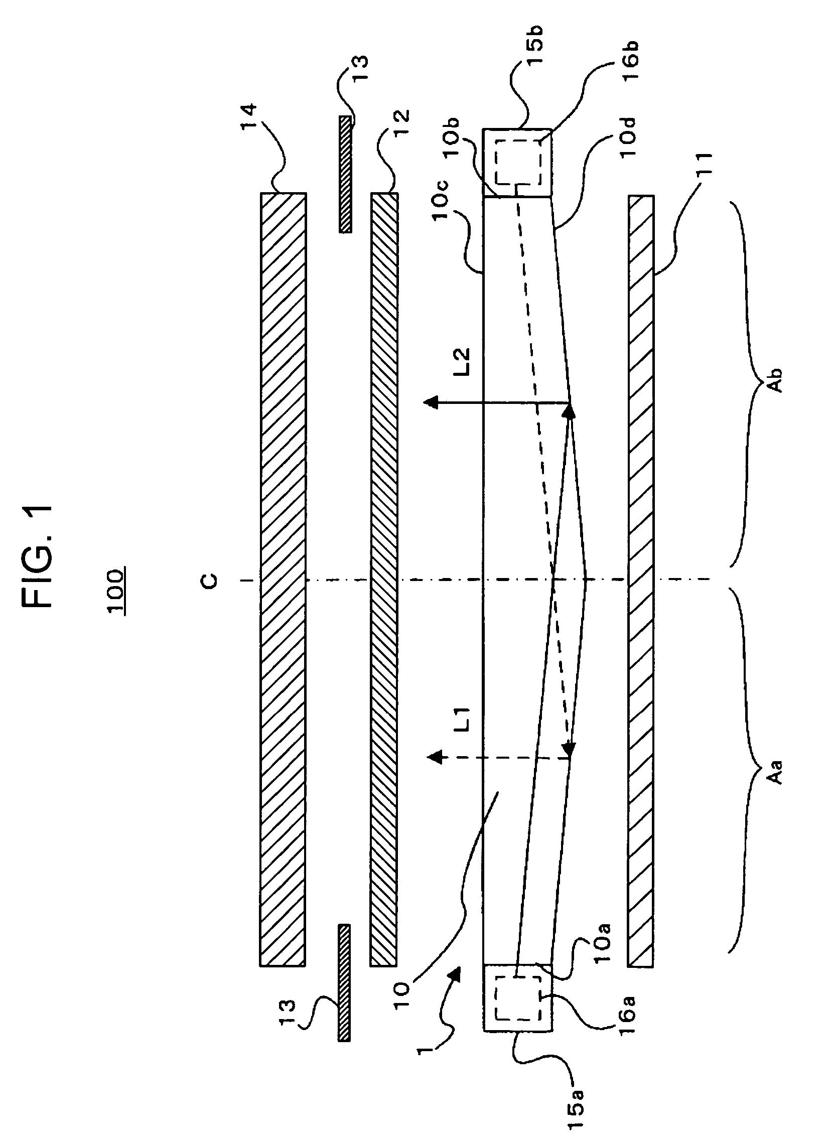
[0037]FIG. 1 is a lateral view schematically showing the structure of a liquid crystal display device 100 in which an illumination device according to a first embodiment of the invention is applied. Even though individual constituent elements are shown separated by gaps for convenience of description in FIG. 1, actually, they constitute a liquid crystal display device 100 in a state in which they overlap in a vertical direction of the drawing.

[0038]The liquid crystal display device 100 includes an illumination device 1. A diffusion sheet 12 and a liquid crystal display panel 14 are provided on the illumination device 1, and a reflection sheet 11 is provided below the illumination device 1. The liquid crystal display panel 14 corresponds to a display panel of a cellular phone or the like, and an optical waveguide 10 has a display area, which is almost equal to a light-emitting area of the liquid crystal display panel 14. In addition, the structure of the liquid crystal panel in the i...

second embodiment

[0073]Next, an illumination device according to a second embodiment of the invention will be described. In the illumination device according to the first embodiment, the optical waveguide 10 is constructed such that the thickness thereof is the largest at the location of the boundary line C and gradually decreases from the location of the boundary line C toward the light incident end faces located at both ends. In contrast, in the illumination device according to the second embodiment, the optical waveguide is entirely ‘wedge-shaped’ and is formed such that the thickness thereof gradually decreases from one light incident end face toward the other light incident end face. Hereinafter, the illumination device according to the second embodiment will be described with reference to FIG. 6.

[0074]FIG. 6A is a lateral view showing the structure of the illumination device 3 according to the second embodiment of the invention. As shown in FIG. 6A, the illumination device 3 has the wedge-shap...

first modification

[0087]The above-mentioned liquid crystal display device 100 has a structure in which only the diffusion sheet is disposed between the liquid crystal panel and the illumination device. However, according to the structure, the inclination angle α in the illumination device 1, the inclination angles α and α′ in the illumination device 2, and the inclination angles α, α1, and α2 in the illumination device 3 are respectively set in a range of 35° to 50°, because it is necessary for the light to be emitted in a substantially vertical direction from the optical waveguide. For this reason, it is required that the reflective surface of the optical waveguide has a relatively steep shape in each of the illumination devices 1 to 3. Therefore, in the first modification, a prism sheet is disposed between the liquid crystal panel and the diffusion sheet in the liquid crystal display device 100. The prism sheet has a surface with unevenness of which the section is substantially triangular formed th...


PUM


Abstract

An illumination device includes an optical waveguide that has light incident end faces formed at both ends thereof; and light sources that are disposed on the light incident end faces formed at both ends of the optical waveguide. A reflective surface of the optical waveguide has first and second reflective surfaces intersecting at a predetermined boundary line, and a light-emitting surface of the optical waveguide has first and second regions divided by the predetermined boundary line. When the light sources provided at one end of the optical waveguide are turned on, light is emitted such that one of the first and second regions is brighter than the other.

Description

RELATED APPLICATIONS[0001]This application claims priority to Japanese Patent Application No. 2004-273077 filed Sep. 21, 2004 which is hereby expressly incorporated by reference herein in its entirety.BACKGROUND OF THE INVENTION[0002]1. Technical Field[0003]The present invention relates to an illumination device, such as a backlight unit used for a liquid crystal display of a cellular phone, and to an optical waveguide for the same.[0004]2. Related Art[0005]In liquid crystal display devices, a backlight unit is provided on a rear surface of a liquid crystal display panel in order to perform transmissive display. Generally, the backlight unit is composed of an illumination device which includes alight source, an optical waveguide for radiating light emitted from the light source onto a rear surface of the liquid crystal display panel as planar light, a diffusion sheet for diffusing the light emitted from the optical waveguide, and a prism sheet for condensing the light.[0006]As a cel...

Claims


Application Information

Patent Timeline
Patent Type & Authority Patents(United States)
IPC IPC(8): F21V7/04
CPCG02B6/0046G02B6/0068G02F1/133606G02F2001/133391G02F2001/133607G02F2001/133626H04M1/0233H04M2250/16H04W52/027G02F1/133391G02F1/133607G02F1/133626Y02D30/70G02F1/1335
Inventor ONISHI, YASUNORI
Owner BOE TECH GRP CO LTD
Why Eureka
Try Eureka