Semiconductor device with intermediate connector

a technology of semiconductor devices and connectors, applied in the direction of individual semiconductor device testing, semiconductor/solid-state device testing/measurement, instruments, etc., can solve the problems of uneven height of 2-level protruding bumps and lack of evenness at the head end section

Inactive Publication Date: 2007-07-24
PANASONIC CORP
View PDF27 Cites 20 Cited by
  • Summary
  • Abstract
  • Description
  • Claims
  • Application Information

AI Technical Summary

Benefits of technology

[0015]It is an object of the present invention to electrically connect with high reliability a semiconductor element with electrodes disposed at a narrow pitch to a circuit substrate by conductive paste.
[0016]According to the present invention, an intermediate connector is provided between a semiconductor section and a circuit substrate. Via holes are formed in the intermediate connector. Because inside each via hole, the conductive paste are sealed in to secure electrical connections between the semiconductor section and the circuit substrate, the conductive paste would not spread from the each via hole to the outside. Consequently, shorting of adjoining electrical connections can be prevented. Further, semiconductor elements with electrodes disposed at a narrow pitch and circuit substrates can be electrically connected with high reliability by conductive paste.
[0017]The conductive paste is used for electrical connections between the semiconductor section and the circuit substrate. Thus, concentration of the stress applying only to the joining section of the semiconductor section and the circuit substrate can be relaxed. Consequently, stable electrical connections can be achieved with respect to dimensional changes caused by thermal shocks, etc.
[0025]The first affixing process and the second affixing process may bring the intermediate connector in close contact with the semiconductor section and the circuit substrate by pressurizing and include a sealing process which seals the each via hole.

Problems solved by technology

Under this condition, the heights of the 2-level protruded bumps are not uniform and the evenness at the head end section also lacks.
This causes problems particularly when the clearances between electrodes 903 and electrodes 913 are narrow.

Method used


Image

  • Semiconductor device with intermediate connector
  • Semiconductor device with intermediate connector
  • Semiconductor device with intermediate connector

Examples


embodiment 1

[0056]FIG. 3A is a cross-sectional diagram showing the overall construction of semiconductor device 100 according to Embodiment 1. Semiconductor element 100 comprises semiconductor element 101, intermediate connector 107, circuit substrate 113, and a plurality of electric connections 120.

[0057]Semiconductor element 101 is an element mounted to circuit substrate 113 and is electrically and physically connected to circuit substrate 113 via each electrical connection 120.

[0058]Circuit substrate 113 is a resin multilayer circuit substrate in which all the layers have an interstitial via hole (IVH) construction. Circuit substrate 113 has a plurality of via holes 119 at optional positions of core 123 that forms an insulation layer. FIG. 3B is a partial enlarged view of semiconductor device 100. By filling conductor 125 in via holes 119, conductivity across wiring layers 121 provided on the front surface and the rear surface of core 123, respectively, is secured. The use of a resin multila...

embodiment 2

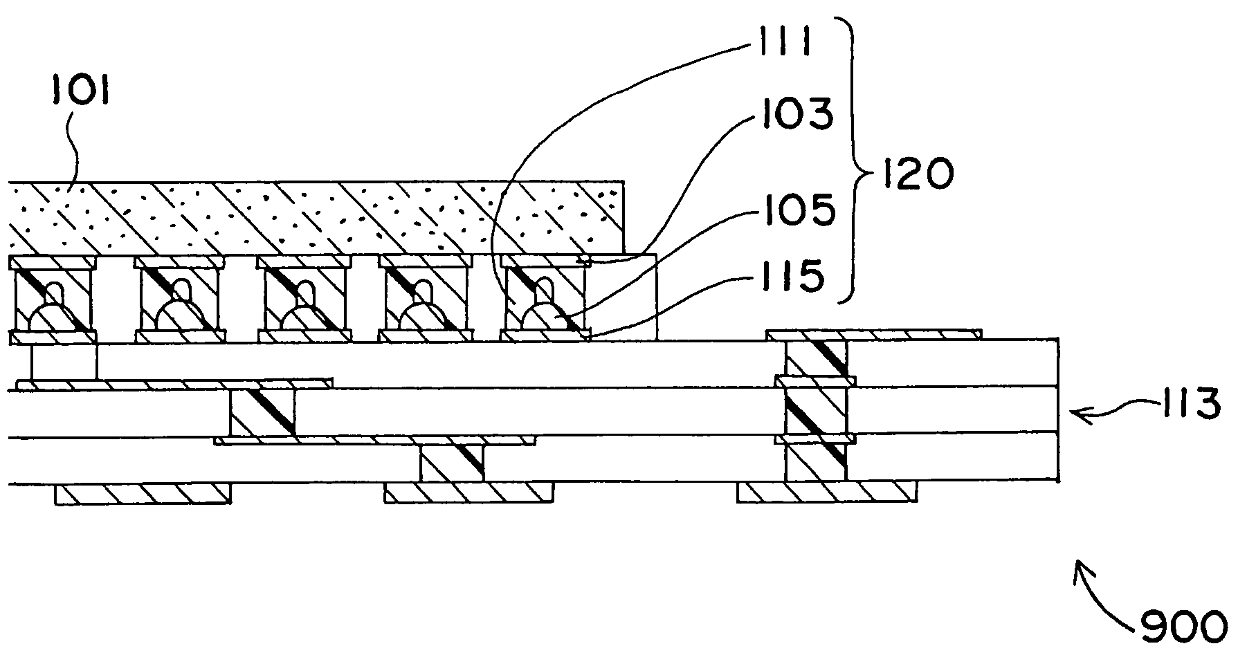
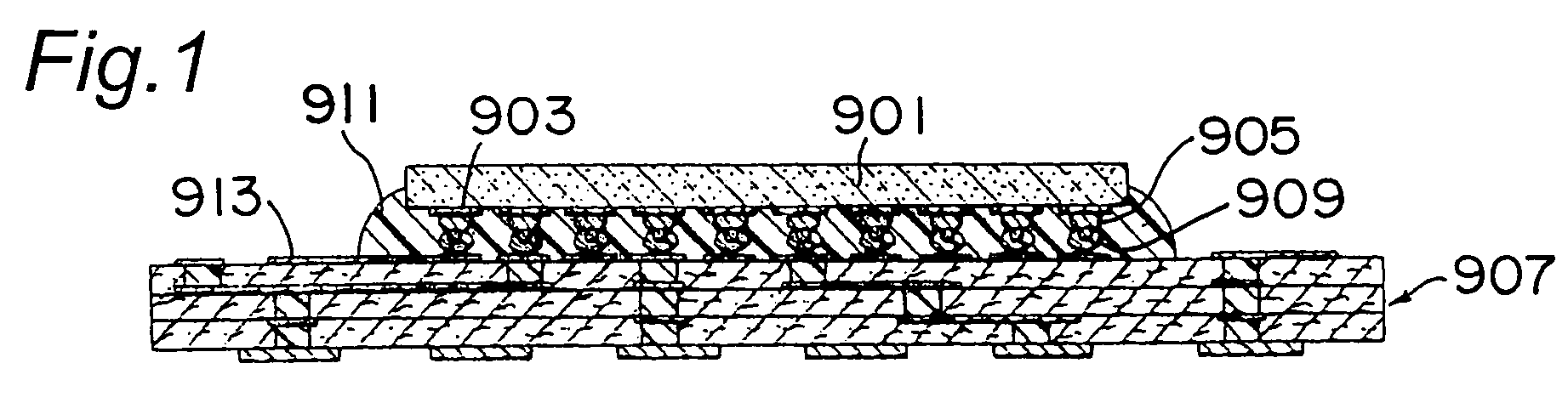
[0111]FIG. 11A is a cross-sectional view showing the construction of semiconductor device 900 according to embodiment 2. FIG. 11B is a partial enlarged view of semiconductor device 900. In embodiment 1, on electrode 103 of semiconductor element 101 (FIG. 3B), bump 105 is provided. Semiconductor device 900 according to the present embodiment has bump 105 provided on electrode 115 of circuit substrate 113. Other configurations, for example, that electrode 103 on semiconductor element 101 and electrode 115 on circuit substrate 113 are electrically connected via bump 105 and conductive paste 111 and that the wall surface of via hole 109 suppresses the flowout of conductive paste 111 and prevents defective shorting across adjoining electrical connections 120, are same as embodiment 1.

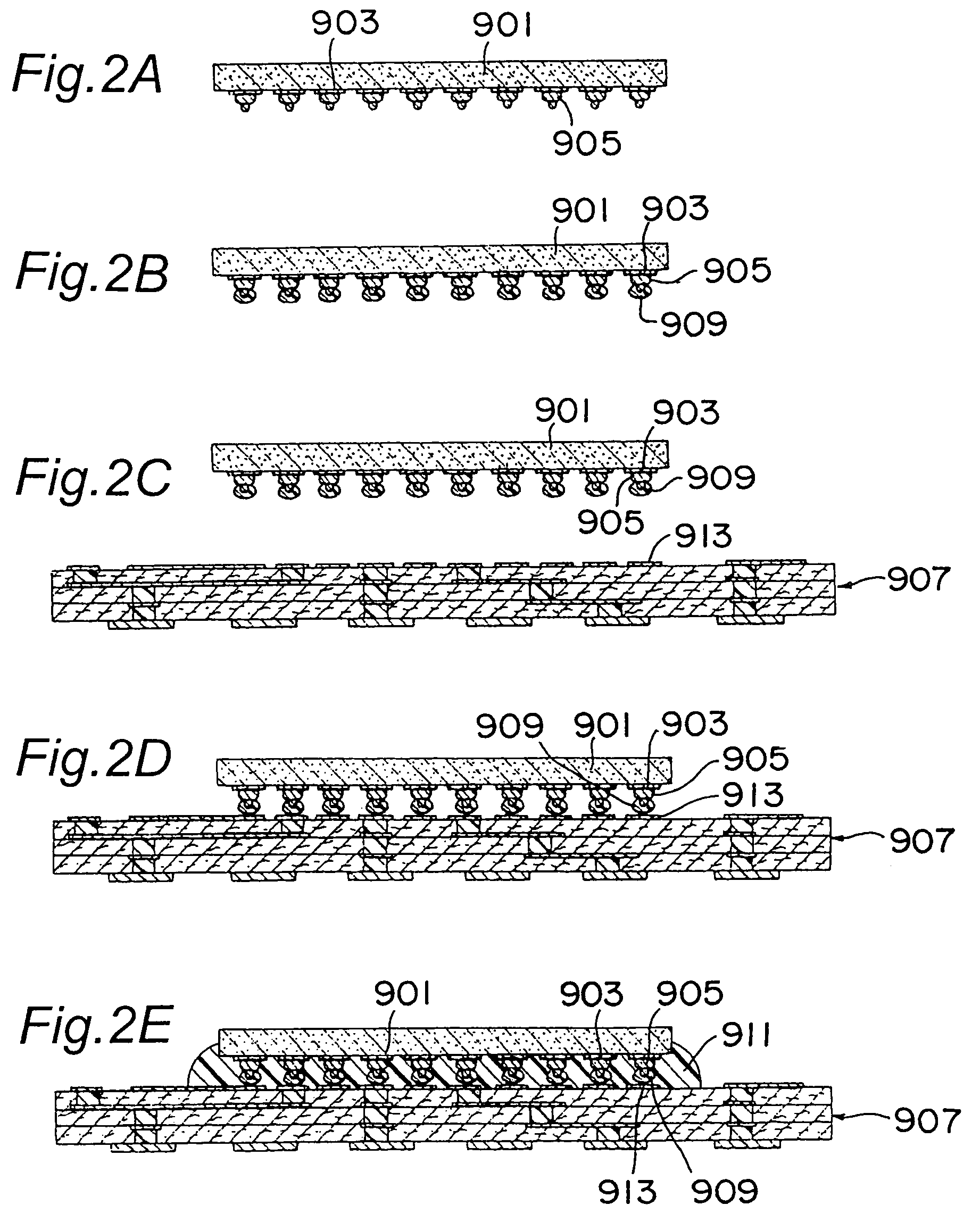
[0112]Referring now to FIG. 12A through 12F, the manufacturing process of semiconductor device 900 (FIG. 11A) according to embodiment 2 is described. First of all, FIG. 12A is a diagram showing circuit subst...

embodiment 3

[0121]FIG. 14 is a cross-sectional view showing the overall construction of semiconductor device 1200 according to embodiment 3. Semiconductor device 1200 is composed with semiconductor element 101 in semiconductor device 100 (FIG. 3A) replaced with packaged structure 805 of semiconductor element.

[0122]Semiconductor device 1200 comprises packaged structure 805, intermediate connector 107, circuit substrate 113, and electrical connections 130. Intermediate connector 107 and circuit substrate 113 are same as embodiments 1 and 2 and detailed description will be omitted.

[0123]Packaged structure 805 has circuit substrate 802, semiconductor element 801 mounted on it, metal wire 803 for electrically connecting circuit substrate 802 and semiconductor element 801, and mold resin 806 provided on the surface of circuit substrate 802 in such a manner to cover semiconductor element 801 and metal wire 803.

[0124]In this embodiment, packaged structure 805 for packaging semiconductor element 801 sec...


PUM


Abstract

A semiconductor element and a circuit substrate each having electrodes disposed at narrow pitch are electrically connected with high reliability by conductive paste. A semiconductor device with a semiconductor section and a circuit substrate electrically connected and a method for manufacturing such semiconductor device are provided. The manufacturing method includes processes of: forming semiconductor electrodes at the semiconductor section; forming substrate electrodes at the circuit substrate; firstly affixing one part of the semiconductor section and circuit substrate to an intermediate connector made of insulating material; forming via holes at intermediate connector according to positions of the semiconductor electrodes and positions of the substrate electrodes; electrically connecting each semiconductor electrode and each substrate electrode via each via hole; and secondly affixing the other part of the semiconductor section and circuit substrate to the intermediate connector.

Description

[0001]This application is a divisional of application Ser. No. 10 / 131,992, filed Apr. 25, 2002, now abandoned.BACKGROUND OF THE INVENTION[0002]1. Field of the Invention[0003]The present invention relates to a technology for mounting semiconductor elements to a circuit substrate at a high density.[0004]2. Description of Background Arts[0005]The packaging density of semiconductor elements has been remarkably increased. In order to meet a decrease in packaging area and an increase in number of electrodes, various high-density packaging methods have been proposed in recent years. As one example, there is a method for facedown-mounting semiconductor elements with bumps formed at the electrode section to circuit substrates (U.S. Patent Publication No. 4,661,192, Laid-open Japanese patent publication No. 6-224259). FIG. 1 is a cross-sectional view of a conventional semiconductor device facedown-mounted.[0006]The conventional semiconductor device shown in FIG. 1 comprises a semiconductor el...

Claims


Application Information

Patent Timeline
Patent Type & Authority Patents(United States)
IPC IPC(8): H01L21/66H01L21/48H01L21/56H01L23/498H05K3/28H05K3/32H05K3/38
CPCH01L21/4853H01L21/563H01L23/49811H01L24/11H01L24/12H01L24/16H01L24/83H01L24/90H05K3/321H01L24/29H01L24/32H01L2224/1134H01L2224/1147H01L2224/13082H01L2224/13144H01L2224/13147H01L2224/1329H01L2224/133H01L2224/16225H01L2224/32225H01L2224/48091H01L2224/48227H01L2224/73203H01L2224/73204H01L2224/73265H01L2224/83101H01L2224/83102H01L2224/83136H01L2224/83192H01L2224/83194H01L2224/838H01L2224/92125H01L2224/92247H01L2924/01005H01L2924/01013H01L2924/01018H01L2924/01029H01L2924/0103H01L2924/01033H01L2924/01046H01L2924/01047H01L2924/01078H01L2924/01079H01L2924/01082H01L2924/0781H01L2924/15311H05K3/28H05K3/388H05K2201/09472H05K2201/10378H05K2201/10674H05K2203/0361H01L2224/16237H01L2224/81191H01L2224/81141H01L24/48H01L2224/2919H01L2224/83851H01L2924/00013H01L2924/01006H01L2924/01024H01L2924/014H01L2924/0665H01L2224/81903H01L2224/1131H01L2924/0132H01L2224/45144H01L2224/11822H01L2224/11902H01L2224/29076H01L2224/2929H01L2224/293H01L2224/325H01L2224/9211H01L2224/13018H01L2924/00014H01L2224/13099H01L2924/00012H01L2924/00H01L2924/3512H01L24/03H01L24/05H01L24/45H01L24/73H01L2224/05568H01L2224/05573H01L2924/12042H01L2924/181H01L2224/05624H01L2224/05644H01L2224/05647H01L2224/05655
Inventor HIGASHITANI, HIDEKINAKAMURA, TADASHIANDOH, DAIZO
Owner PANASONIC CORP
Why Eureka
Try Eureka