Semiconductor device

a semiconductor and device technology, applied in static indicating devices, instruments, optics, etc., can solve the problems of electrostatic discharge damage easily induced, degradation or destruction of a semiconductor element connected damage to the pixel electrode, so as to increase the capacitance of the capacitor element, reduce the luminance of the light emitting element due to variations in the characteristics of driving transistors, and improve image quality

Inactive Publication Date: 2007-07-24
SEMICON ENERGY LAB CO LTD
View PDF16 Cites 23 Cited by
  • Summary
  • Abstract
  • Description
  • Claims
  • Application Information

AI Technical Summary

Benefits of technology

[0009]In view of the foregoing, the invention provides a semiconductor device including a light emitting element, in which electrostatic discharge damage during manufacturing steps is prevented. More specifically, the invention prevents electrostatic discharge damage of a semiconductor device in which manufacturing steps up to the formation of a pixel electrode are completed.
[0021]The invention adopting the aforementioned structures provides a semiconductor device in which variations in luminance of light emitting elements due to variations in characteristics of driving transistors are reduced and image quality is thus enhanced, while not increasing capacitance of a capacitor element provided between a gate and a source of a driving transistor or lowering off-current of a switching transistor.

Problems solved by technology

In particular, during manufacturing steps involving charged particles, such as dry etching and electron beam evaporation, the pixel electrode functions as an antenna and thus electrostatic discharge damage is easily induced.
Sudden discharge of electric charges that have built up in the pixel electrode leads to degradation or destruction of a semiconductor element connected to the pixel electrode.
Further, when transporting a substrate in which manufacturing steps up to the formation of a pixel electrode are completed, the pixel electrode on the substrate is exposed, and therefore, electrostatic discharge damage may be caused via the pixel electrode in the case where static electricity occurs during transporting the substrate.
However, increasing the capacitance while lowering the off-current is difficult in manufacturing steps.

Method used


Image

  • Semiconductor device
  • Semiconductor device
  • Semiconductor device

Examples


embodiment mode 1

[Embodiment Mode 1]

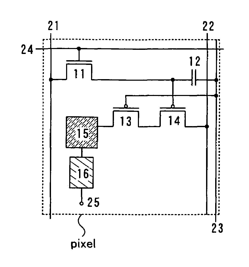
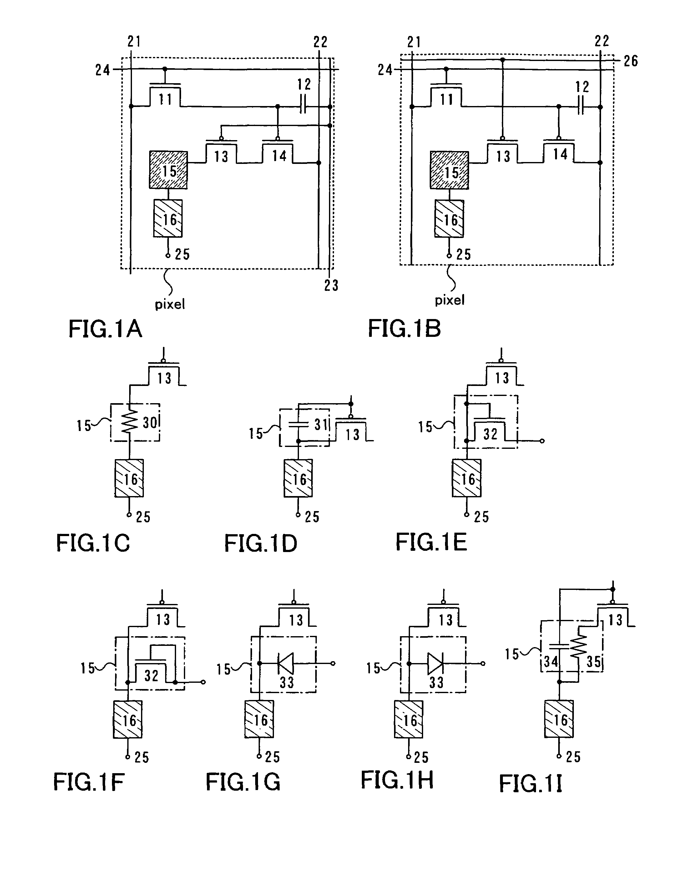
[0043]A circuit configuration of a pixel included in the semiconductor device of the invention is described with reference to FIGS. 1A to 11. A pixel shown in FIG. 1A comprises a signal line 21 and power supply lines 22 and 23 arranged in columns and a scan line 24 arranged in rows. The pixel also comprises a switching transistor 11 (hereinafter referred to as a transistor 11), a driving transistor 13 (hereinafter referred to as a transistor 13), a current controlling transistor 14 (hereinafter referred to as a transistor 14), a protection means 15, and a light emitting element 16. One electrode of the light emitting element 16 is connected to a counter power supply 25.

[0044]A pixel shown in FIG. 1B has the same configuration as that in FIG. 1A, except that a gate electrode of the transistor 13 is connected to a power supply line 26 arranged in rows. That is, the pixels shown in FIGS. 1A and 1B show the same equivalent circuit diagram. However, in the case where t...

embodiment mode 2

[Embodiment Mode 2]

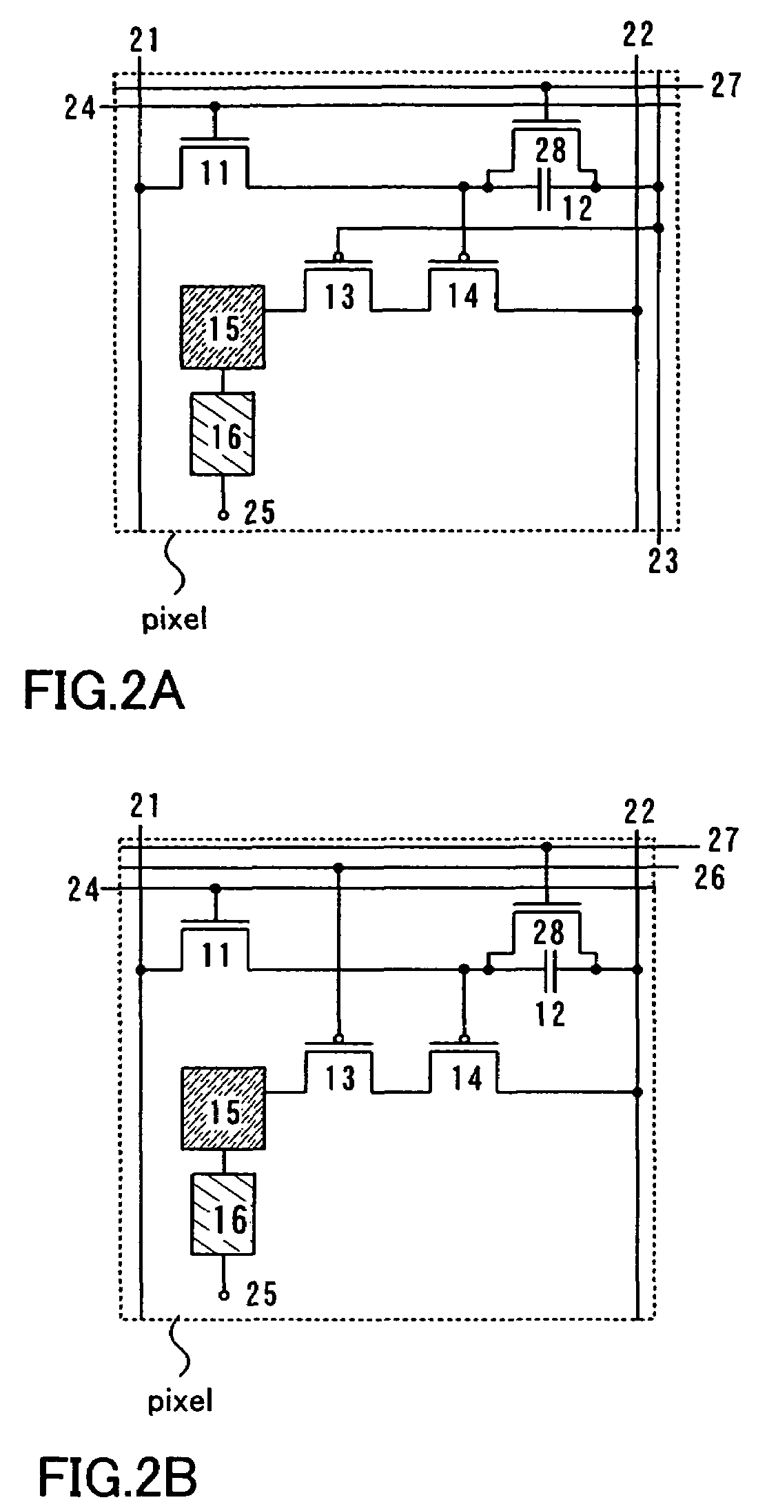
[0056]A circuit configuration of a pixel included in the semiconductor device of the invention is described with reference to FIGS. 2A and 2B. A pixel shown in FIG. 2A comprises the signal line 21 and the power supply lines 22 and 23 arranged in columns, and the scan line 24 and a scan line 27 arranged in rows. The pixel further comprises the transistor 11, the transistor 13, the transistor 14, an erasing transistor 28 (hereinafter referred to as a transistor 28), a capacitor element 12, the protection means 15, and the light emitting element 16. One electrode of the light emitting element 16 is connected to the counter power supply 25.

[0057]The pixel shown in FIG. 2A has the same configuration as that shown in FIG. 1A, except that the transistor 28 and the scan line 27 are additionally provided, therefore, detailed description thereof is omitted herein. Similarly, a pixel shown in FIG. 2B has the same configuration as that shown in FIG. 1B, except that the transi...

embodiment mode 3

[Embodiment Mode 3]

[0060]A light emitting element has a structure in which an electro luminescent layer is sandwiched between a pair of electrodes. More specifically, an electro luminescent layer is formed on a patterned first conductive layer (first electrode), and a second conductive layer (second electrode) is formed so as to cover the whole surface of the electro luminescent layer. In this case, heat treatment is preferably performed on the second conductive layer formed over the electro luminescent layer in order to lower the resistance. However, the electro luminescent layer has a low heat resistance and can not withstand heat treatment at a high temperature. Therefore, due to different resistance values, a voltage applied between a pair of electrodes may differ between in the edges and the center of the light emitting element, which may result in degraded image quality and increased power consumption. In view of this problem, an auxiliary conductive layer (wiring) is connecte...


PUM


Abstract

A semiconductor device in which electrostatic discharge damage during manufacturing steps is prevented. More specifically, a semiconductor device in which electrostatic discharge damage during a step in which the formation of a pixel electrode is completed is prevented. A semiconductor device of the invention comprises a light emitting element, a driving transistor and a protection means disposed between the light emitting element and the driving transistor. The protection means comprises as least one of a resistor element, a capacitor element and a rectifier element. More specifically, the protection means is disposed between a pixel electrode of the light emitting element and a source electrode or a drain electrode of the driving transistor. It is to be noted that the rectifier element is an element having a rectifying function and corresponds to a diode or a transistor whose drain electrode and gate electrode are connected to each other.

Description

BACKGROUND OF THE INVENTION[0001]1. Field of the Invention[0002]The present invention relates to a semiconductor device using a semiconductor element such as a transistor, and more specifically relates to a semiconductor device provided with a protection means in order to prevent electrostatic discharge damage.[0003]2. Description of the Related Art[0004]Static electricity builds up, developing due to friction, contact and the like with air and objects such as conductors, semiconductors and insulators. When there are an excess of charges on these materials, electrostatic discharge is caused, and in the case where this condition occurs on a free node such as an input terminal, minute semiconductor elements formed on a substrate are degraded or destroyed. This is referred to as electrostatic discharge damage. In order to prevent such electrostatic discharge damage, a circuit formed on a substrate (hereinafter referred to as an internal circuit) is connected to an external IC (hereinaf...

Claims


Application Information

Patent Timeline
Patent Type & Authority Patents(United States)
IPC IPC(8): G09G3/10G09G3/20G09G3/30G09G3/32H01L21/822H01L27/04H01L27/32H01L29/786
CPCG09G3/3233G09G3/3275H01L27/3244H01L27/3248G09G3/2022G09G2300/0426G09G2300/0465G09G2300/0842G09G2300/0861G09G2310/061G09G2320/0223G09G2320/0233G09G2320/043G09G2330/04G09G2330/06H01L27/3276G02F1/136204H10K59/123H10K59/131H10K59/1315H10K59/12
Inventor OSAME, MITSUAKIANZAI, AYAYAMAZAKI, YU
Owner SEMICON ENERGY LAB CO LTD
Why Eureka
Try Eureka