

Probe station with low inductance path
a probe station and low inductance technology, applied in the field of probe stations, can solve the problems of exhibiting significant inductance to high current measurements of existing probe stations, and achieve the effect of reducing the number of inductance of existing probe stations
- Summary
- Abstract
- Description
- Claims
- Application Information
AI Technical Summary
Benefits of technology
Problems solved by technology
Method used
Image

Examples
Embodiment Construction
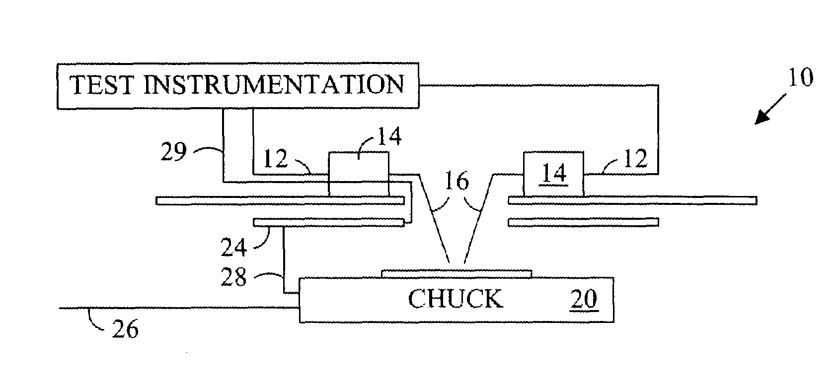
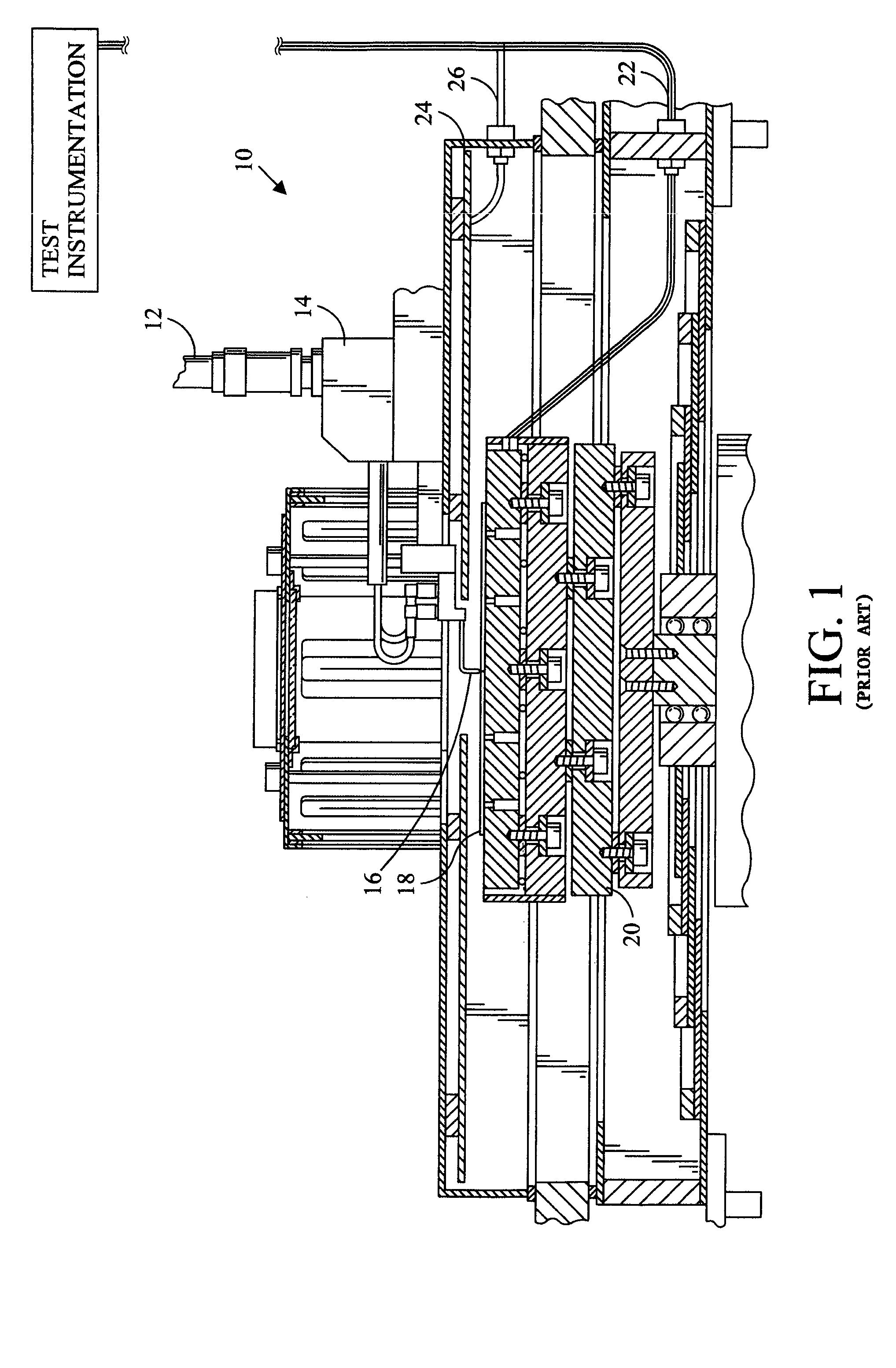
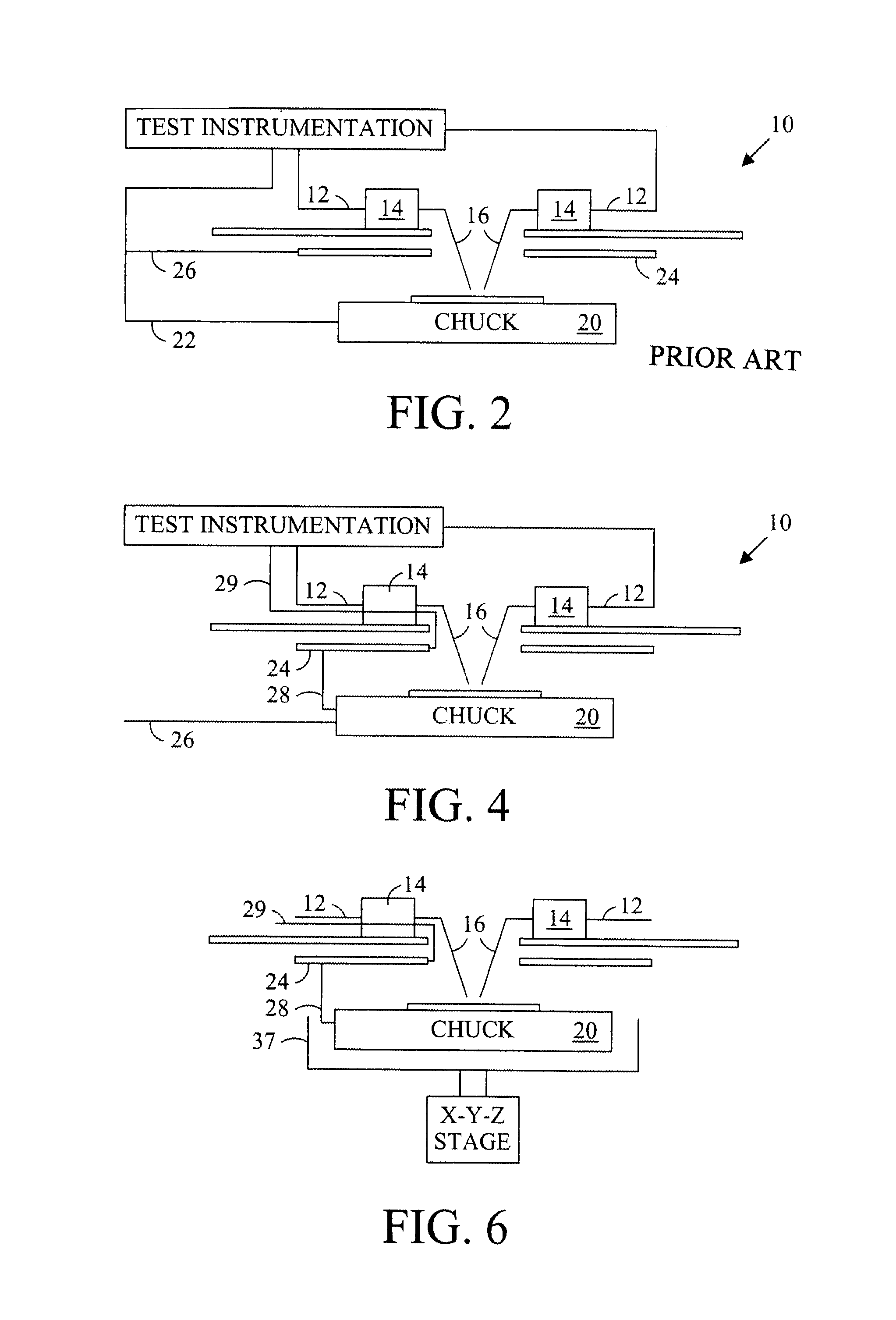
[0017]FIG. 1 shows a general schematic diagram of an existing probe station 10 having guard and electromagnetic shield structures. A test signal is provided through a test path 12 to a probe 14 having probe needles 16 that contact an electrical device 18 resting upon a chuck 20. The probe needles may alternatively be any type of contacts, such as for example, probe cards, probes on movable positioners, optical signals, and membrane probes. The chuck 20 receives a guard signal through a first transmission line 22 while a suspended guard member 24 receives a guard signal through a second transmission line 26. The first transmission line 22 likewise includes a test signal path to the chuck 20. The first transmission line 22, the test path 12, the probe 14, the needles 16, the device 18, and the chuck 20 together form a large loop, as shown in FIG. 1, to a common signal source at the test instrumentation. Normally within the probe station the transmission line 22 is within a service loo...
PUM
 Abstract
Description
Claims
Application Information