Nonvolatile memory with multi-frequency charge pump control

a non-volatile memory and charge pump technology, applied in the direction of digital storage, semiconductor devices, instruments, etc., can solve the problems of shortened deterioration of load drivability, and erroneous so as to improve communication distance of ic cards and stabilize operation of ic cards

Active Publication Date: 2007-07-31
RENESAS ELECTRONICS CORP
View PDF6 Cites 29 Cited by
  • Summary
  • Abstract
  • Description
  • Claims
  • Application Information

AI Technical Summary

Benefits of technology

[0019]An object of the invention is to provide a technique capable of performing stable communications with increased communication distance in an IC card by suppressing a peak current at the time of operation of a boosting circuit provided for an EEPROM.
[0027](1) Since the current peak when the voltage generator operates can be reduced, the peak in consumption current in the semiconductor integrated circuit device can be suppressed.
[0028](2) from (1), by constructing an IC card by using the semiconductor integrated circuit device of the invention, at the time of transmitting information via an information transmission medium such as electric waves, the communication distance of the IC card can be increased or the operation of the IC card can be stabilized.

Problems solved by technology

The inventors herein, however, found that the IC cards have the following problems.
As the communication distance increases, the load drivability deteriorates.
It may cause erroneous operation in the IC card or the like.
Consequently, there is a problem such that, to obtain sufficient load drivability, the communication distance of the IC card is shortened.

Method used


Image

  • Nonvolatile memory with multi-frequency charge pump control
  • Nonvolatile memory with multi-frequency charge pump control
  • Nonvolatile memory with multi-frequency charge pump control

Examples


Embodiment Construction

[0040]Embodiments of the invention will be described in detail hereinbelow with reference to the drawings. In all of the drawings for explaining the embodiments, as a principle, the same reference numerals are designated to the same members and their repetitive description will not be given.

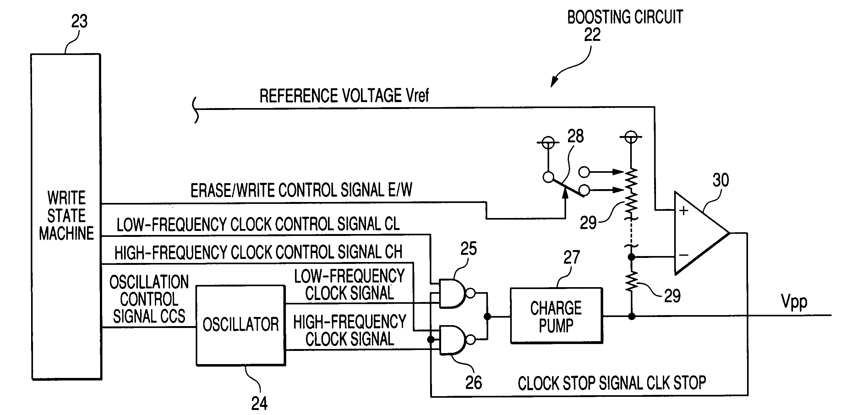
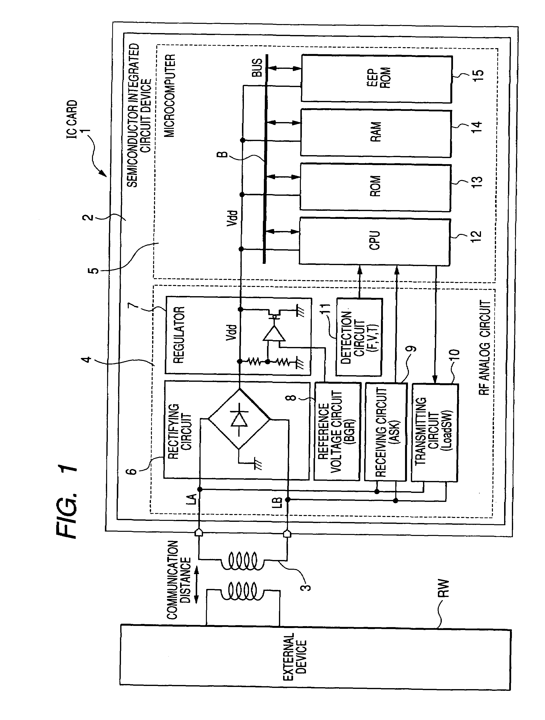
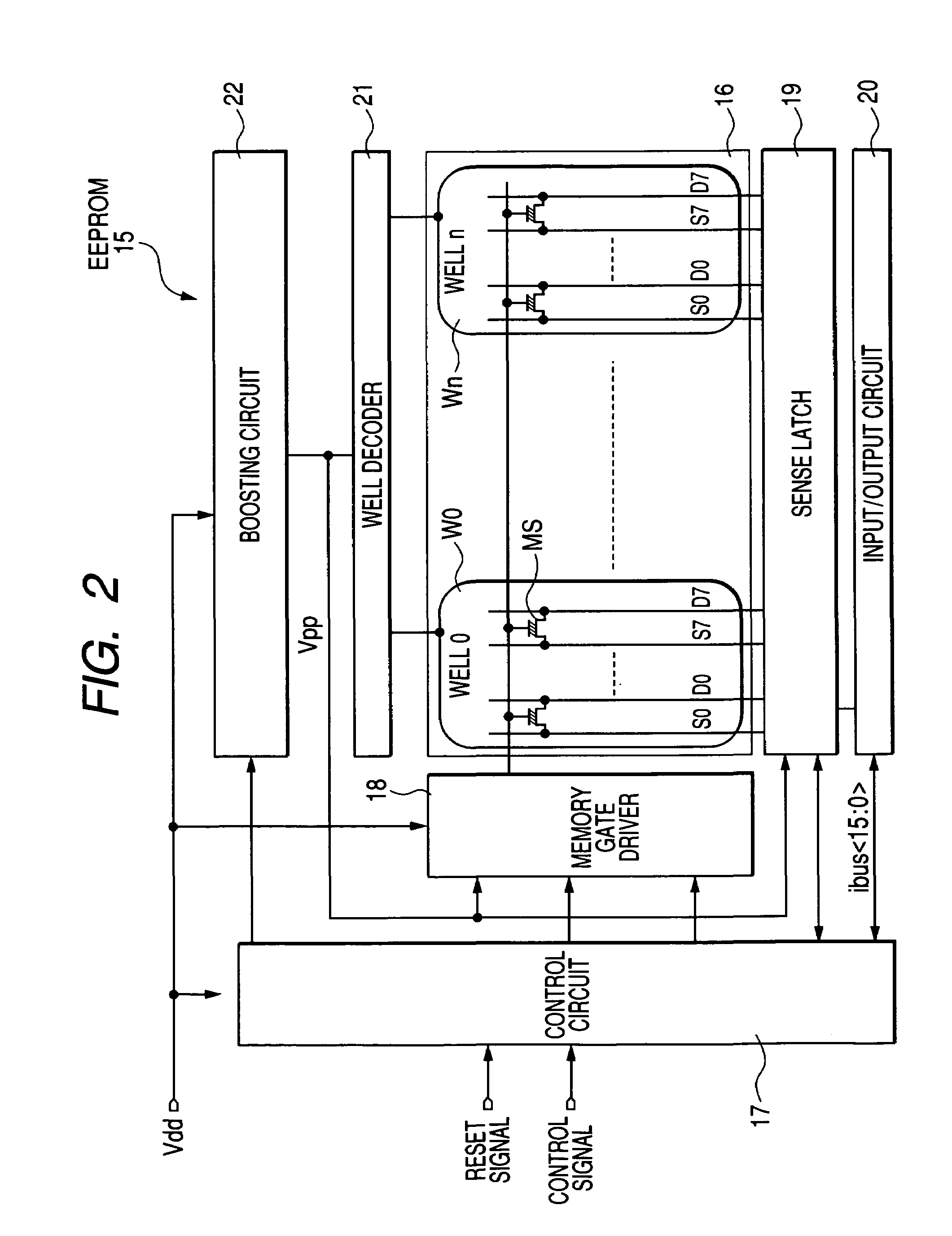
[0041]FIG. 1 is a block diagram of an IC card according to an embodiment of the invention. FIG. 2 is a block diagram showing a semiconductor integrated circuit device provided for the IC card in FIG. 1. FIGS. 3A and 3B are diagrams illustrating the relations of voltages of components applied to memory cells at the erasure and write times in an EEPROM provided for the semiconductor integrated circuit device in FIG. 2. FIG. 4 is a block diagram showing an example of a boosting circuit provided for the EEPROM in FIG. 2. FIG. 5 is a timing chart showing operation waveforms of parts in the boosting circuit in FIG. 4. FIG. 6 is a diagram showing operation waveforms of a selection clock signal and boost...


PUM


Abstract

The present invention is directed to largely reduce peak current at the time of operation of a boosting circuit provided for an EEPROM. In the erase / write operation, first, a low-frequency clock signal as a selection clock signal is input by a low-frequency clock control signal to a charge pump. After lapse of a certain period (about ⅓ of fall time), a high-frequency clock signal having a frequency higher than that of the low-frequency clock signal is output by a high-frequency clock control signal and is input as the selection clock signal to the charge pump to boost a voltage to a predetermined voltage level. In such a manner, while suppressing the peak of consumption current, the fall time of the boosted voltage can be shortened.

Description

CROSS-REFERENCE TO RELATED APPLICATION[0001]The present application claims priority from Japanese patent application No. 2004-130710 filed on Apr. 27, 2004, the content of which is hereby incorporated by reference into this application.BACKGROUND OF THE INVENTION[0002]The present invention relates to a voltage boosting technique in a semiconductor memory and, more particularly, to a technique effective when applied to control of a boosted voltage in an EEPROM (Electrically Erasable and Programmable Read Only Memory).[0003]In recent years, an IC card having the functions of a credit card and a telephone card is being spread. The IC card is a card having a shape similar to that of a magnetic card and on which a CPU and a memory are mounted. Reading / writing on the memory is controlled by the CPU. The card itself has a ciphering function and therefore has a high security function and large storage capacity.[0004]There are IC cards of a contact type having, as one of means for transmitti...

Claims


Application Information

Patent Timeline
Patent Type & Authority Patents(United States)
IPC IPC(8): G11C16/04H01L27/04G11C5/14G11C7/00G11C16/12H01L21/822H03K5/08
CPCG11C5/145G11C16/12
Inventor KAWAJIRI, YOSHIKITERASAWA, MASAAKIYAMAZOE, TAKANORI
Owner RENESAS ELECTRONICS CORP
Why Eureka
Try Eureka