Gas injection apparatus for semiconductor processing system

a technology of gas injection apparatus and semiconductor, applied in vacuum evaporation coating, chemical vapor deposition coating, coating, etc., can solve the problems of showerhead type gas injection apparatus, inapplicability to magnetron sputtering system, and difficulty in optimizing these systems for a wide range of gas pressure and flow rate, and achieve high level uniformity

Inactive Publication Date: 2007-08-07
SAMSUNG ELECTRONICS CO LTD
View PDF7 Cites 226 Cited by
  • Summary
  • Abstract
  • Description
  • Claims
  • Application Information

AI Technical Summary

Benefits of technology

[0026]Through the above configurations, the present invention may achieve at least one of the following: high level uniformity in gas flow rates by and adaptation to various kinds of semiconductor processing systems including plasma processing systems and magnetron sputtering systems irrespective of the size of the reaction chamber, gas pressure and flow rate.

Problems solved by technology

This gas injection apparatus may be effective in achieving the gas distribution uniformity, but is likely to prohibit ion flux flowing to the substrate due to the portions of nozzles extending toward the interior of the reaction chamber.
However, it is very difficult to optimize these systems for a wide range of gas pressures and flow rates.
Another drawback is that the showerhead type gas injection apparatus is suitable only for a parallel plate plasma reactor and cannot be applicable to magnetron sputtering systems.
In this manner, a conventional ring-shaped gas injection apparatus makes gas pressure and flow rate at each nozzle extremely nonuniform due to differences in the lengths of gas paths connecting a gas inlet to each nozzle through a gas channel.
Despite this structural requirement for a gas channel having a small sectional area, a large gas injection apparatus with a thin gas channel still has a problem with uniform pressure distribution.
Accordingly, as wafer sizes continue to increase, ensuring even gas distribution to the reaction chamber with a conventional gas injection apparatus becomes more difficult.
This deteriorates uniformity across a semiconductor substrate being processed, which in turn significantly worsens the quality and yield of semiconductor devices.

Method used


Image

  • Gas injection apparatus for semiconductor processing system
  • Gas injection apparatus for semiconductor processing system
  • Gas injection apparatus for semiconductor processing system

Examples


first embodiment

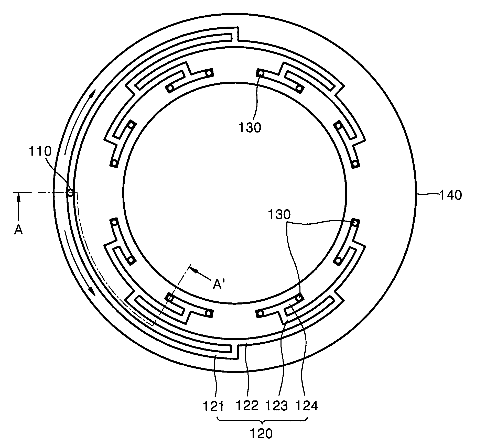
[0047]The gas injection apparatus according to this invention includes a gas inlet 110 penetrating an upper wall 182 of the reaction chamber 180 and a flat ring-shaped injector 140 attached to the bottom of the upper wall 182 of the reaction chamber 180. The injector 140 has a manifold 120 including gas channels 121-124, arranged on a plurality of levels and a plurality of nozzles 130. The gas channels 121-124 are sequentially arranged on different levels on the top surface of the injector 140 so that the gas channel 121 is closest to the outer circumference of the injector 140 and the gas channel 124 is closest to the inner circumference of the injector 140. The detailed configuration, operation, and effects of the gas injection apparatus are as described above.

[0048]The injector 140 of the gas injecting apparatus according to this invention is inserted into a groove 182a formed in the bottom of the upper wall 182 of the reaction chamber 180. Thus, since there is no projection towa...

second embodiment

[0049]FIG. 6 shows a gas injection apparatus according to a second embodiment of the present invention. The second embodiment shown in FIG. 6 is an example in which the gas injection apparatus of FIG. 3A is modified to have a cylindrical shape and can be applied to a plasma processing system. The gas injection apparatus according to the present invention includes a gas inlet 210 penetrating a side wall 183 of the reaction chamber 180 and a cylindrical injector 240 attached to the inner surface of the side wall 183 thereof. The injector 240 has a manifold 220 including gas channels 221-224, arranged on a plurality of levels, and a plurality of nozzles 230. The injector 240 may be inserted into a groove 183a formed in the inner surface of the sidewall 183 of the reaction chamber 180.

[0050]The gas channels 221-224 may be formed along an outer circumference of the injector 240 in the shape of a groove having a predetermined depth. The gas channels 221 through 224 may be disposed at diff...

third embodiment

[0056]A plurality of levels of gas channels 421-424 constituting a manifold 420 are formed in the shape of a groove having a predetermined depth on a sloped inner surface of the upper wall 282 of the reaction chamber 280 instead of along an outer surface of the injector 440. Otherwise, the arrangement of the gas channels 421-424 is the same as that of the gas channels 321-324 according to the present invention.

[0057]The injector 440 may be formed of a dielectric liner such as ceramic material resistant to sputtering. The injector 440 is useful where the slightest sputtering has a significant adverse effect on semiconductor processing.

[0058]Each of the plurality of nozzles 430 is formed to penetrate the injector 340 from a predetermined location on the outer surface of the injector 440, corresponding to both ends of each of the gas channels 424 at the lowest level toward the interior of the reaction chamber 280. The exits of the plurality of nozzles 430 may be spaced evenly along an ...


PUM

PropertyMeasurementUnit
sizesaaaaaaaaaa
pressureaaaaaaaaaa
lengthaaaaaaaaaa

Abstract

A gas injection apparatus for injecting a reactive gas into a reaction chamber of a semiconductor processing system includes an injector in contact with an inner surface of a wall of the reaction chamber. The injector has a plurality of nozzles through which the reactive gas is injected into the reaction chamber. A gas inlet penetrates the wall of the reaction chamber. A manifold is disposed between the wall of the reaction chamber and the injector, and supplies the reactive gas flowing through the gas inlet to the nozzles. Gas channels in the manifold are arranged on a plurality of levels to equalize the lengths of gas paths connecting the gas inlet to each of the plurality of nozzles. This configuration makes the flow rate of reactive gas supplied through each of the plurality of nozzles to the reaction chamber uniform.

Description

BACKGROUND OF THE INVENTION[0001]1. Field of the Invention[0002]The present invention relates to a semiconductor processing system, and more particularly, to a gas injection apparatus for supplying a reactive gas for processing a semiconductor substrate into a reaction chamber.[0003]2. Description of the Related Art[0004]Semiconductor processing systems such as plasma processing systems or magnetron sputtering systems have been mostly used in a micromachining process performed on a semiconductor substrate for manufacturing a semiconductor device or flat display panel. For example, plasma enhanced chemical vapor deposition (PECVD) systems or high-density plasma CVD (HDP-CVD) systems have been mostly used to deposit a material layer on a substrate by CVD. Magnetron sputtering systems have been widely used to deposit a material layer on a substrate by physical vapor deposition (PVD).[0005]Semiconductor processing systems are being developed that best suit various process characteristic...

Claims


Application Information

Patent Timeline
Patent Type & Authority Patents(United States)
IPC IPC(8): C23C16/00C23F1/00H01L21/306C23C14/34C23C16/44C23C16/455H01L21/203H01L21/205
CPCC23C16/4558H01L21/205
Inventor KIM, TAE-WANTOLMACHEV, YURI NIKOLAEVICHMA, DONG-JOONNAVALA, SERGIY YAKOVLEVICH
Owner SAMSUNG ELECTRONICS CO LTD
Why Eureka
Try Eureka