Flip chip packaging process

a packaging process and flip chip technology, applied in the direction of electrical equipment, semiconductor devices, semiconductor/solid-state device details, etc., can solve the problems of significant difference between the inherent properties of these two materials, become vulnerable to damage, and get deteriorated, so as to increase the available surface area on the substrate and increase the reliability of the flip chip package structure

Active Publication Date: 2007-08-14
ADVANCED SEMICON ENG INC
View PDF3 Cites 19 Cited by
  • Summary
  • Abstract
  • Description
  • Claims
  • Application Information

AI Technical Summary

Benefits of technology

[0011]Accordingly, the present invention is directed to a chip molding process, in which an underfill is used as an encapsulant to reduce the occurrence of delamination after molding process.
[0012]The present invention is also directed to a flip chip molding process, in which the space between chips for cutting a substrate is small so that the usage area on the substrate is increased.
[0017]The flip chip packaging of the invention uses the underfill as the encapsultant, therefore the occurrence of delamination due to differential coefficients of thermal expansion between different materials can be reduced and thus the reliability of the flip chip package structure is increased. Furthermore, the flooding of the encapsulant over the cutting line is not an issue. Therefore, the available area on the substrate is increased, i.e., more chips can be mounted on the substrate.

Problems solved by technology

After the underfill is filled, the chip 110 is exposed from the substrate and thus becomes vulnerable to damage by external forces or get deteriorated by atmospheric dusts or moisture.
Therefore, there is a significant difference between the inherent properties of these two materials.
However, the distance D is limited by the size of the chip in CSP packaging, that is, the area outside the chip bonding area must be less than 20% of total area of all package structures.
Furthermore, since the underfill 130 and the encapsulant 132 are different materials, delamination tends to occur due to the differential coefficients of thermal expansion, and thus the performance of the chip 110 will be deteriorated due to external moisture or temperature change.

Method used


Image

  • Flip chip packaging process
  • Flip chip packaging process
  • Flip chip packaging process

Examples


Embodiment Construction

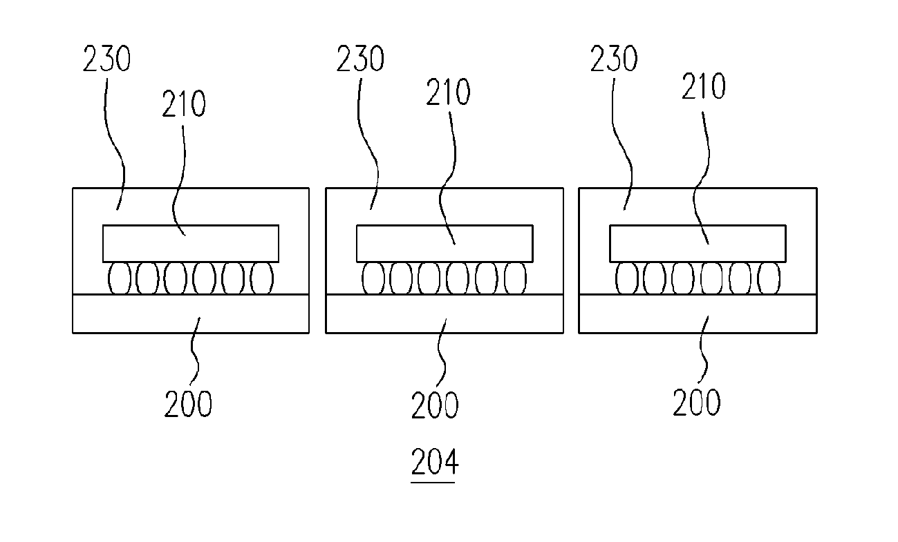
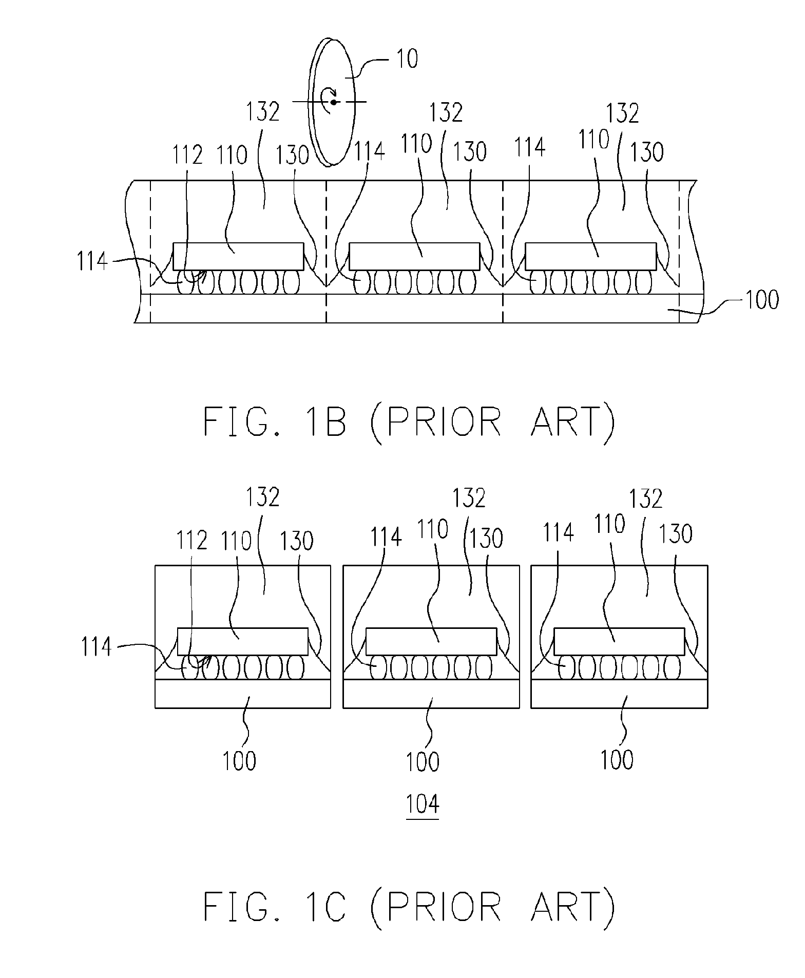
[0020]FIG. 2A-2E are schematic views of a flip chip packaging process according to one embodiment of the invention. Referring to FIG. 2A, a substrate 200 is provided. The substrate 200 has a plurality of substrate units 202 on which a plurality of chips are mounted using a flip chip interconnection technology to form a plurality of chip scale package (CSP) units. The substrate 200 can be, for example, a multiple-layer circuit substrate of which the outermost layer has a plurality of contacts (not shown). Those contacts can be arranged on chip bonding areas (indicated by a slanted area) of the substrate 200 in various manners as intermediates of electrical connection of the substrate 200 to the chips 210.

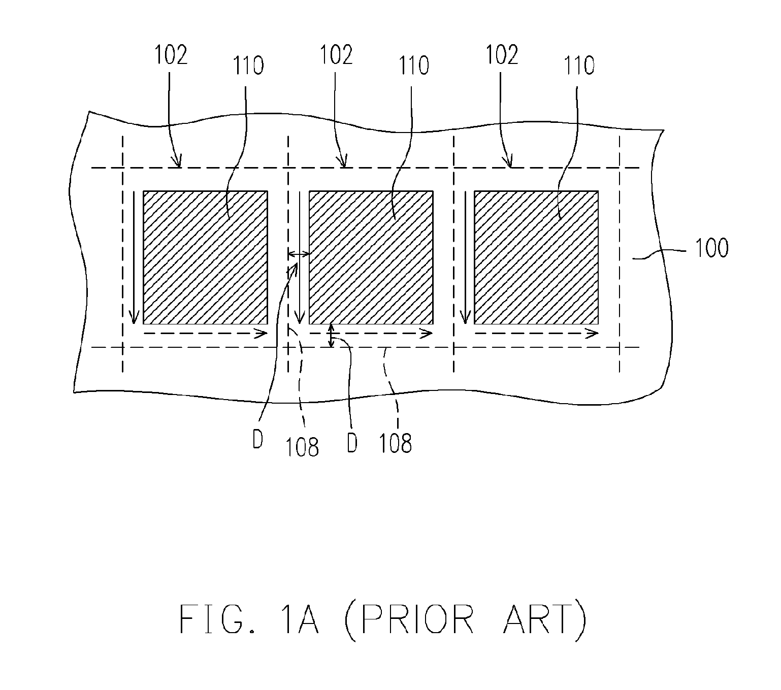
[0021]It is noted that there is a predetermined space between the chips 210 for cutting the substrate 200. The distance D1 between edges of the chips 210 and cutting line 208 is as small as possible, and the whole width of a cutting tool can be accommodated into the distance D1. The ...


PUM


Abstract

A flip chip packaging process uses an underfill as an encapsultant to reduce the possibility of delamination from occurring due to differential coefficients of thermal expansion, and thus the reliability of a flip chip package structure can be increased. Furthermore, the flooding of the encapsulant over the cutting line need not be taken into consideration for cutting the substrate. Therefore, the usage area of the substrate usage is increased, i.e., more chips can be mounted per unit area of the substrate.

Description

CROSS-REFERENCE TO RELATED APPLICATION[0001]This application claims the priority benefit of Taiwan application serial no. 93106613, filed on Mar. 12, 2004.BACKGROUND OF THE INVENTION[0002]1. Field of the Invention[0003]This invention relates to a flip chip packaging process, and more particularly to a packaging process using an underfill as an encapsulant.[0004]2. Brief Description of Related Art[0005]In semiconductor industry, integrated circuit (IC) production includes three stages: wafer production, IC production and IC packaging. Dies are obtained by means of wafer production, circuit design, multiple mask processes and wafer sawing. Each die electrically connects to a carrier via its bonding pads. The carrier can be a packaging substrate or a printed circuit board (PCB). Wires and / or bumps are usually used as intermediate connections between the chip and the carrier. A flip chip interconnection technology may be adapted for fabricating a plurality of bumps in area array on the ...

Claims


Application Information

Patent Timeline
Patent Type & Authority Patents(United States)
IPC IPC(8): H01L21/44H01L23/31
CPCH01L21/561H01L21/563H01L24/97H01L2224/97H01L2224/16225H01L2224/32225H01L2224/73204H01L2224/81H01L2224/83H01L2924/00H01L2924/351H01L2924/15787H01L2924/181H01L2924/14
Inventor CHEN, JIAN-CHENGCHEN, YU-WENWU, SHENG-YU
Owner ADVANCED SEMICON ENG INC
Why Eureka
Try Eureka