Wire bonding on thinned portions of a lead-frame configured for use in a micro-array integrated circuit package

Active Publication Date: 2007-08-21
NAT SEMICON CORP
View PDF20 Cites 24 Cited by
  • Summary
  • Abstract
  • Description
  • Claims
  • Application Information

AI Technical Summary

Problems solved by technology

Current semiconductor packaging technology often involves tradeoffs between ease and efficiency of manufacturing on the one hand, and various performance drawbacks on the other.
However, lead-frame based packages, whose connectors are typically placed either on or extending from the sides, tend to have larger footprints than ball grid array (BGA) packages, whose solder ball connectors lie directly underneath the package.
Unfortunately, BGA packages have drawbacks as well.
Specifically, such packages often employ laminate substrates rather than uniform metal lead-frames, making them more expensive to produce than lead-frame based packages, and less efficiently manufactured.

Method used


Image

  • Wire bonding on thinned portions of a lead-frame configured for use in a micro-array integrated circuit package
  • Wire bonding on thinned portions of a lead-frame configured for use in a micro-array integrated circuit package
  • Wire bonding on thinned portions of a lead-frame configured for use in a micro-array integrated circuit package

Examples


Embodiment Construction

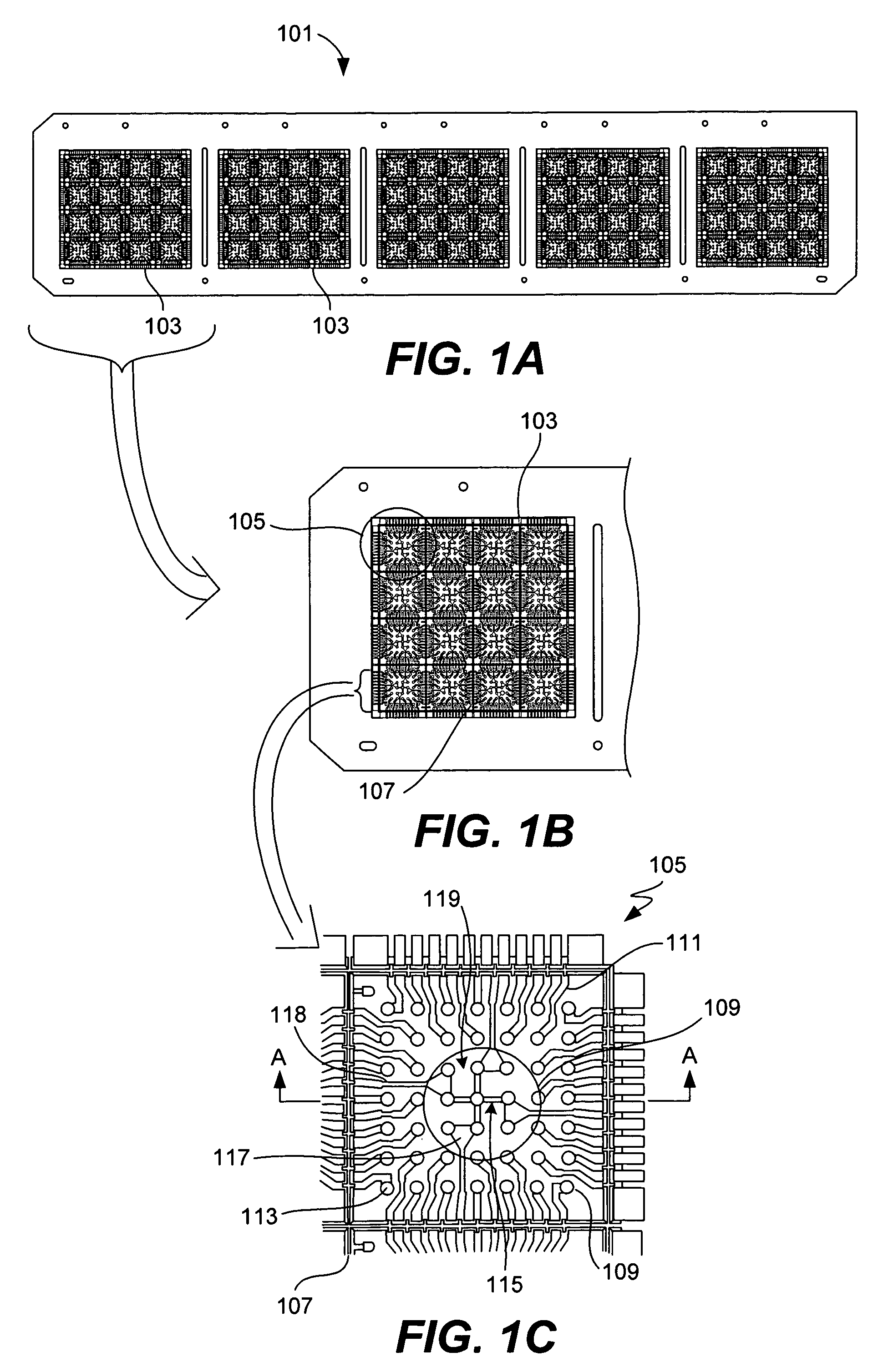
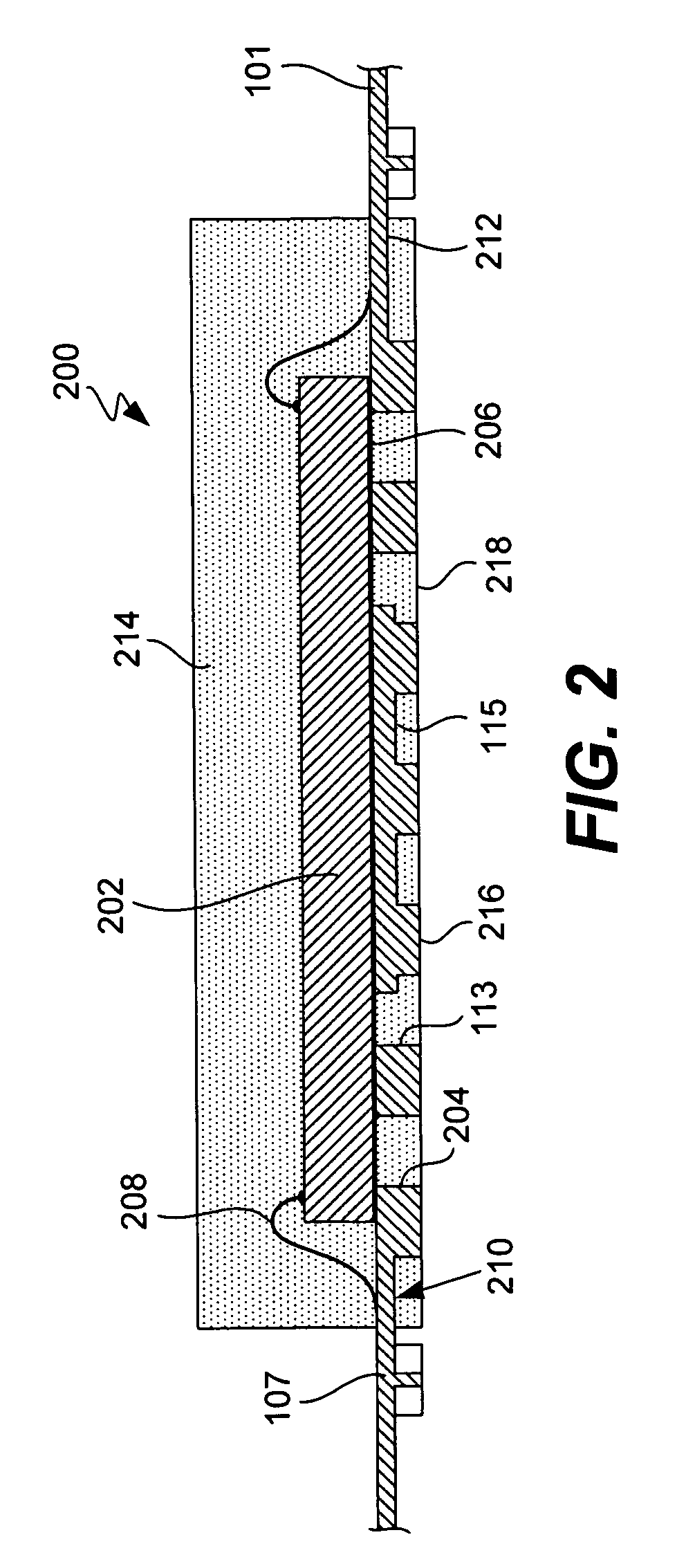
[0020]In one embodiment of the invention, an integrated circuit package is disclosed. The package has solder ball connectors on its lower surface, like conventional BGA packages. However, this package is produced using many features of lead-frame based packages. Such a package utilizes at least four different elements to achieve various improvements over the art. First, a lead-frame is employed with perforated die attach pads that allow encapsulant material to more easily flow underneath the dice, thus preventing process problems such as voids in the encapsulant layer. The drive toward smaller package sizes has also yielded smaller contact pads for placing solder ball connectors. As reductions in contact pad area also reduce the strength with which solder balls adhere to the package, a second improvement involves square contact pads that retain the same metal-to-metal clearance as standard circular contact pads, but that have a greater surface area. In this manner, embodiments of th...


PUM


Abstract

Aspects of the invention recite wire bonding on thinned portions of a lead-frame that is configured for use in an IC package. A harder lead-frame material, improved adhesive tape, and various structural features of the lead-frame itself, in various combinations or subcombinations, facilitate the attachment of wire bonds to thinned areas of the lead-frame. This eliminates the need for supports placed directly under the bond sites, removing unwanted conductive areas on the outer surface of an IC package.

Description

BRIEF DESCRIPTION OF THE INVENTION[0001]This invention relates to the packaging of integrated circuits (ICs). More specifically, this invention relates to the design and fabrication of a micro-array IC package.BACKGROUND OF THE INVENTION[0002]Current semiconductor packaging technology often involves tradeoffs between ease and efficiency of manufacturing on the one hand, and various performance drawbacks on the other. For example, lead-frame based packages such as quad flat no-lead (QFN) packages employ lead-frames to facilitate the packaging and singulation of multiple units at once. However, lead-frame based packages, whose connectors are typically placed either on or extending from the sides, tend to have larger footprints than ball grid array (BGA) packages, whose solder ball connectors lie directly underneath the package. Unfortunately, BGA packages have drawbacks as well. Specifically, such packages often employ laminate substrates rather than uniform metal lead-frames, making ...

Claims


Application Information

Patent Timeline
IPC IPC(8): H01L23/34
CPCH01L21/568H01L23/3107H01L23/49541H01L23/49548H01L24/97H01L2224/32245H01L2224/48091H01L2224/48247H01L2224/73265H01L2224/97H01L2924/01013H01L2924/01029H01L2924/01078H01L2924/01079H01L2924/01082H01L2224/85H01L24/48H01L2924/01005H01L2924/01006H01L2924/01033H01L2924/01074H01L2224/48465H01L2924/00012H01L2924/00H01L24/73H01L2924/14H01L2924/181H01L2924/00014H01L2224/45099H01L2224/45015H01L2924/207
Inventor BAYAN, JAMIE A.PRABHU, ASHOK S.YEEN, CHAN PENGRAMLEY, HASFIZANADARAJAH, SANTHIRAN S/O
Owner NAT SEMICON CORP
Why Eureka
Try Eureka