
Flash memory device with reduced access time

a flash memory and access time technology, applied in the field of semiconductor devices, can solve the problems of reducing the performance of the overall system, increasing processing time, and complicated algorithms, and achieve the effect of simplifying the design algorithm and reducing the access tim

Inactive Publication Date: 2007-08-21
SK HYNIX INC
View PDF9 Cites 18 Cited by
  • Summary
  • Abstract
  • Description
  • Claims
  • Application Information

AI Technical Summary

Benefits of technology

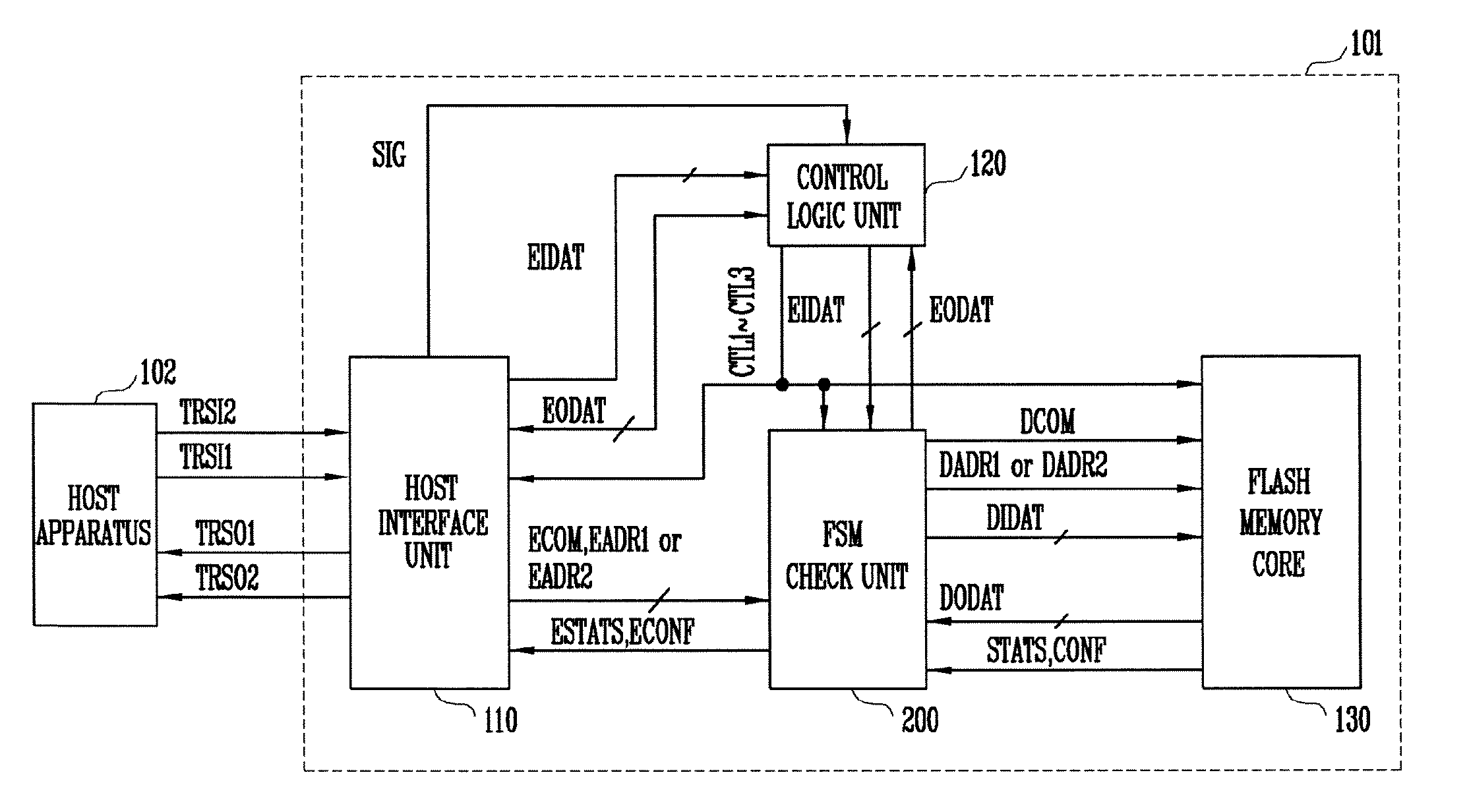
The patent describes a flash memory device that uses a simplified design algorithm and reduces access time by performing error detection and correction operations while encoding or decoding transmission and reception signals with a host apparatus. The device includes a FSM check unit and a flash memory core. The FSM check unit detects and corrects errors in input data signals, command signals, write address signals, and read address signals, and decodes any of these signals. The flash memory core stores the decoded data signals, outputs the read data signals, and outputs the state information and chip information. The technical effect of this invention is to improve the speed and reliability of flash memory devices by reducing access time and errors.

Problems solved by technology

Therefore, when they are designed by Very-High-speed integrated circuit Hardware Description Language (VHDL) or Velilong Hardware Description Language, a problem arises because an algorithm becomes complicated.
This results in an increased processing time.
Therefore, from a viewpoint of the host apparatus 20, a problem arises because the performance of an overall system is lowered since the access time of the flash memory device 10 is increased.

Method used


Image

  • Flash memory device with reduced access time
  • Flash memory device with reduced access time
  • Flash memory device with reduced access time

Examples


Embodiment Construction

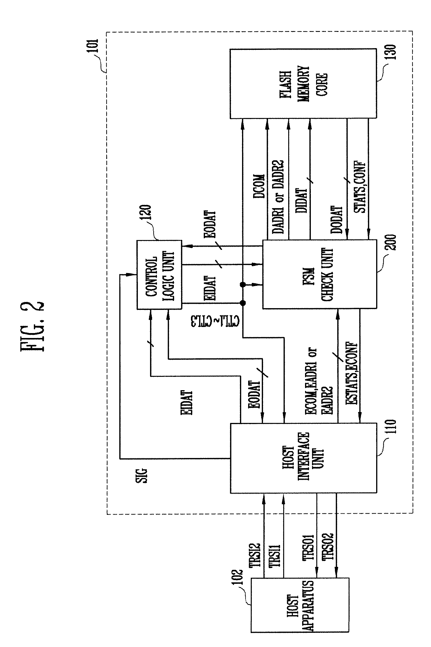
[0012]FIG. 2 is a block diagram of a flash memory device. Referring to FIG. 2, the flash memory device 101 may include a host interface unit 110, a control logic unit 120, a flash memory core 130 and a FSM check unit 200.

[0013]The host interface unit 110 interfaces the control logic unit 120 and the FSM check unit 200, and an external host apparatus 102. More particularly, the host interface unit 110 can extract a command signal (ECOM), an input data signal (EIDAT) and a write address signal (EADR1) or a command signal (ECOM) and a read address signal (EADR2) from a first transmission signal (TRSI1) received from the host apparatus 102. The command signal (ECOM) may include a program command or a read command. The host interface unit 110 outputs the input data signal (EIDAT) to the control logic unit 120 and outputs the command signal (ECOM) and the write or read address signal (EADR1 or EADR2) to the FSM check unit 200. Furthermore, the host interface unit 110 extracts a control in...


PUM


Abstract

A flash memory device with a reduced access time. The flash memory device executes an error detection and correction operation while encoding or decoding transmission and reception signals with a host apparatus. The flash memory device utilizes a simplified design algorithm and reduces an access time.

Description

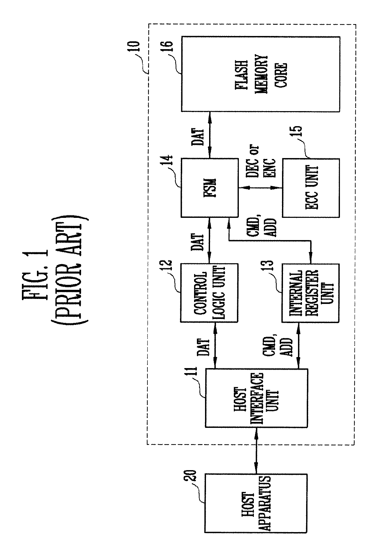
TECHNICAL FIELD[0001]This patent relates to semiconductor devices, and more particularly, to flash memory devices.DISCUSSION OF RELATED ART[0002]In general, in a system including a flash memory device, the flash memory device functions to store various data received from a host apparatus (or a control apparatus), read data requested by the host apparatus and transmit the read data to the host apparatus. For data transmission with the host, the flash memory device includes an encoding and decoding unit such as a finite state machine (FSM). A typical flash memory device including the FSM is shown in FIG. 1.[0003]Referring to FIG. 1, the flash memory device 10 includes a host interface unit 11, a control logic unit 12, an internal register unit 13, a FSM 14, an Error Correction Code (ECC) unit 15 and a flash memory core 16.[0004]The FSM 14 decodes a data signal (DAT) received from the control logic unit 12 and a command signal (CMD) and an address signal (ADD) received from the interna...

Claims


Application Information

Patent Timeline
Patent Type & Authority Patents(United States)
IPC IPC(8): G11C11/34
CPCG06F11/1068G11C7/1006G11C2029/0411A61G17/08A61G17/007B65D2585/00
Inventor YOU, BYOUNG SUNG
Owner SK HYNIX INC
Learn More