Die pad for semiconductor packages and methods of making and using same

a technology of semiconductor packages and die pads, which is applied in the direction of semiconductor devices, semiconductor/solid-state device details, electrical devices, etc., can solve the problems of insufficient strength of half-etched steps or reentrant portions on the side surfaces of die pads to retain die pads, insufficient size or length of half-etched steps or reentrant portions to thoroughly prevent moisture from permeating into the vicinity of semiconductor chips, etc., to facilitate the egress of moisture from the package

Inactive Publication Date: 2007-08-28
ADVANCED INTERCONNECT TECH LTD
View PDF8 Cites 88 Cited by
  • Summary
  • Abstract
  • Description
  • Claims
  • Application Information

AI Technical Summary

Benefits of technology

[0015]In any of the embodiments, the die pad may further include tie bars extending therefrom, and at least one lip may extend from a side surface of the die pad. Also, at least one aperture may extend from the first side of the die pad to the second side of the die pad, with the semiconductor device spanning the at least one aperture for facilitating the egress of moisture from the package.
[0019]In any of the embodiments, the die pad may further include tie bars extending therefrom, and the method may further include: etching a portion of a surface of the tie bar coplanar with the first surface of the die pad to form a surface of the tie bar offset from the first surface of the die pad. The method may also include forming at least one lip at a side surface of the die pad. Also, at least one aperture may extend from the first side of the die pad to the second side of the die pad, with the semiconductor device spanning the at least one aperture for facilitating the egress of moisture from the package.

Problems solved by technology

However, because the die pad is exposed at a surface of the package, there is no molding compound to support the exposed surface of the die pad, and steps must be taken to ensure that the die pad does not become dislodged from the package.
While the solutions described in the '981 and '568 patents are acceptable for certain applications, they are not without their deficiencies.
For example, the half-etched steps or reentrant portions on the side surfaces of the die pad may not be sufficiently robust to retain the die pad within the package under certain conditions or for certain applications.
In another example, as described in U.S. Pat. No. 6,525,406, which is incorporated by reference herein in its entirety, the size or length of this half-etched step or reentrant portion is insufficient to thoroughly prevent moisture from permeating into the vicinity of the semiconductor chip.
The moisture may then spread widely over the inside of the semiconductor package, resulting in cracking of the semiconductor package or causing protuberances to form on the surface of the semiconductor package.
While this solution is effective in increasing the moisture-permeation path of the finished package, half-etching the perimeter of both the upper and lower surface of the die pad results in a very thin protrusion (relative to the thickness of the die pad) extending around the perimeter of the die pad, which may break during fabrication or use of the package.

Method used


Image

  • Die pad for semiconductor packages and methods of making and using same
  • Die pad for semiconductor packages and methods of making and using same
  • Die pad for semiconductor packages and methods of making and using same

Examples


first embodiment

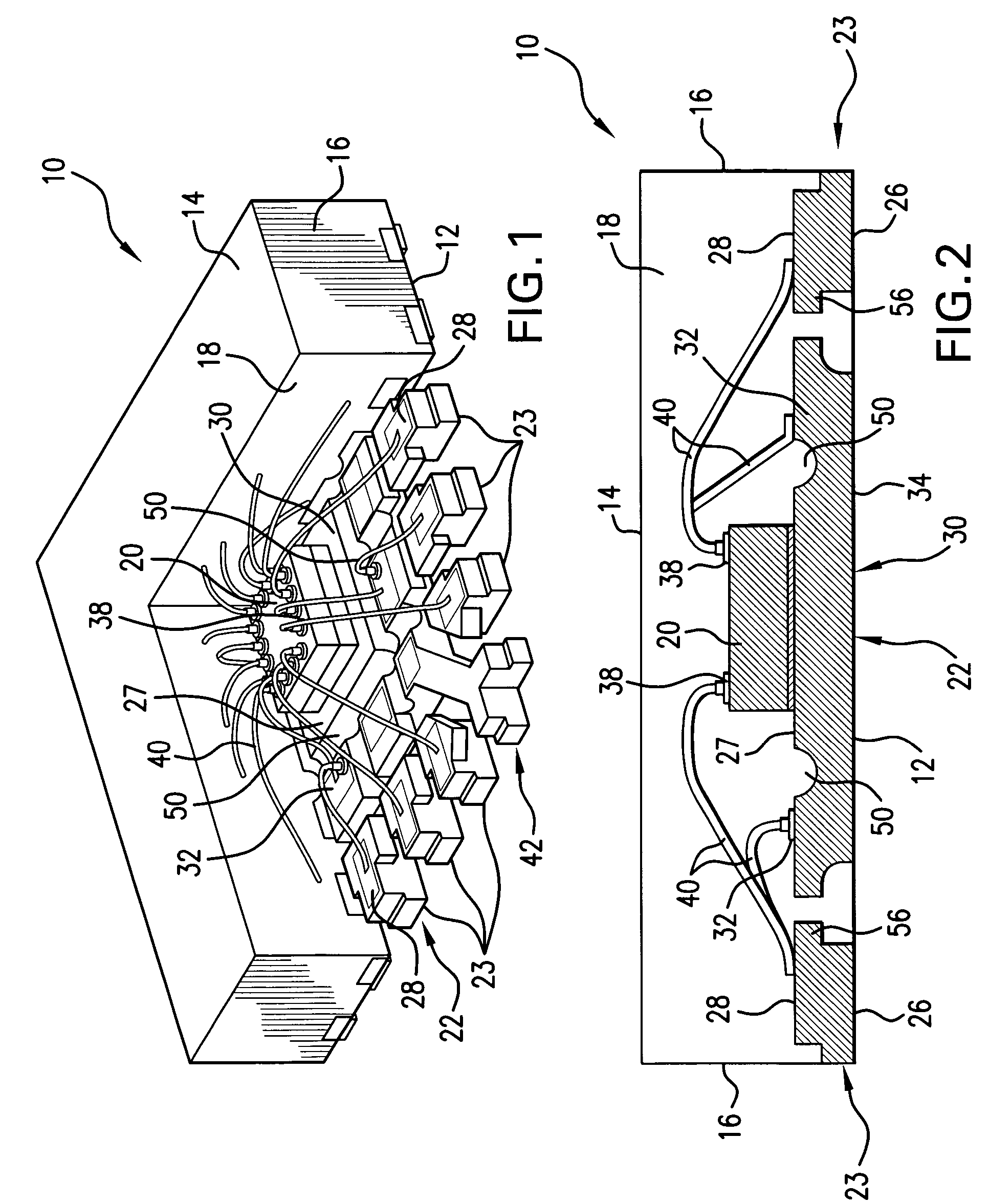
[0042]FIG. 1 is a partial cut-away, top perspective view of a quad, no-lead, wirebonded semiconductor device package 10 in accordance with the present invention, and FIG. 2 is a cross-sectional elevation view of the semiconductor device package 10. Referring to FIGS. 1 and 2, the semiconductor device package 10 has a bottom (first) package face 12, a top (second) package face 14 opposite the bottom package face 12, and package side faces 16 extending between the bottom and top package faces 12, 14. The various package faces are formed in part by a molding compound 18, which covers a semiconductor device (die) 20 and portions of an electrically conductive lead frame 22. The electrically conductive lead frame 22 includes a plurality of leads 23. Each of the leads 23 has a first lead surface 26 disposed at the bottom package face 12 and a bond site 28 opposite the first lead surface 26. In the embodiment shown, the bond sites 28 are electrically connected to associated input / output I / O...

second embodiment

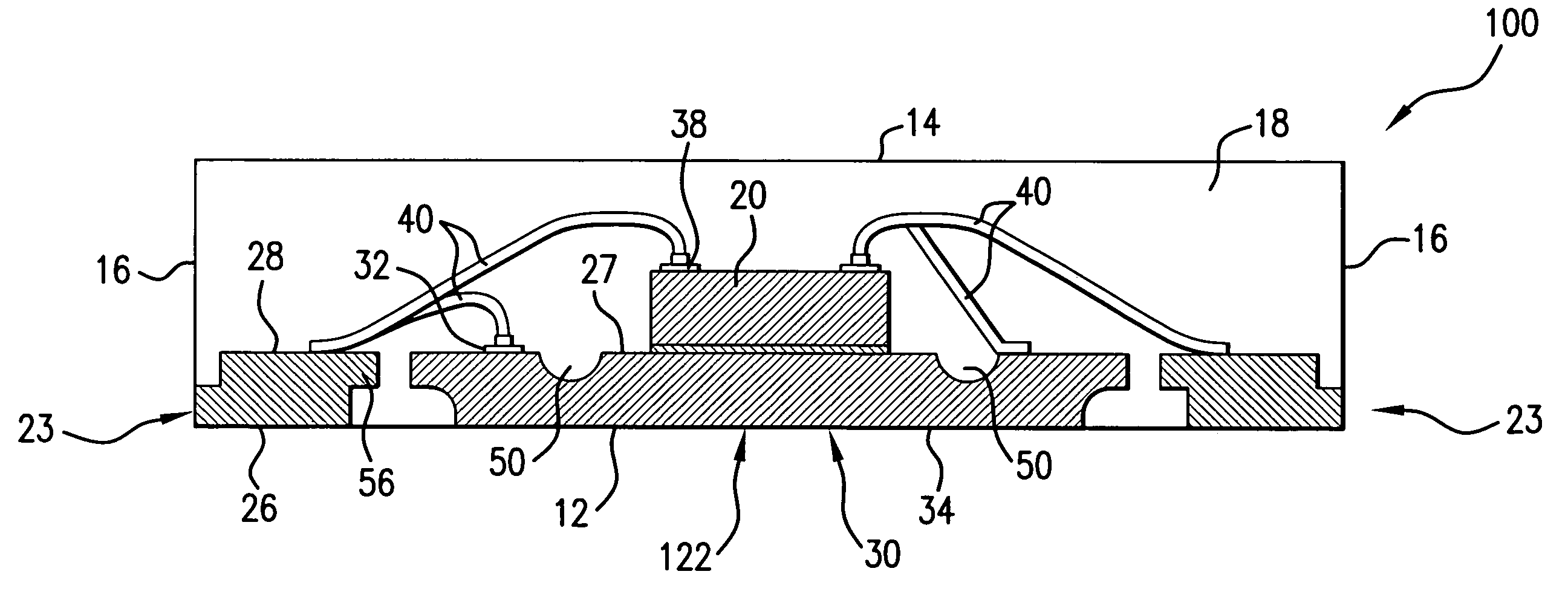
[0061]It is contemplated that the die pad 30 may incorporate any one or both of the roughened surface 27 and the grooves 50, 52, with or without the use of lips 44 and tie bars 42. For example, FIG. 7 is a partial cut-away, top perspective view of a quad, no-lead, wirebonded semiconductor device package 100 in accordance with the present invention, and FIG. 8 is a cross-sectional elevation view of the semiconductor device package 100. The package 100 of FIGS. 7 and 8 is substantially similar to the package 10 shown in FIGS. 1-6, except that the lead frame 122 in package 100 does not include lips 44 protruding from the sides of the die pad 30, as found in the lead frame 22 of package 10. Like the lead frame 22, the lead frame 122 includes a roughened surface 27 and channels 50 and 52 disposed in the die pad 30, which are effective in securing the die pad 30 to the molding compound 18.

third embodiment

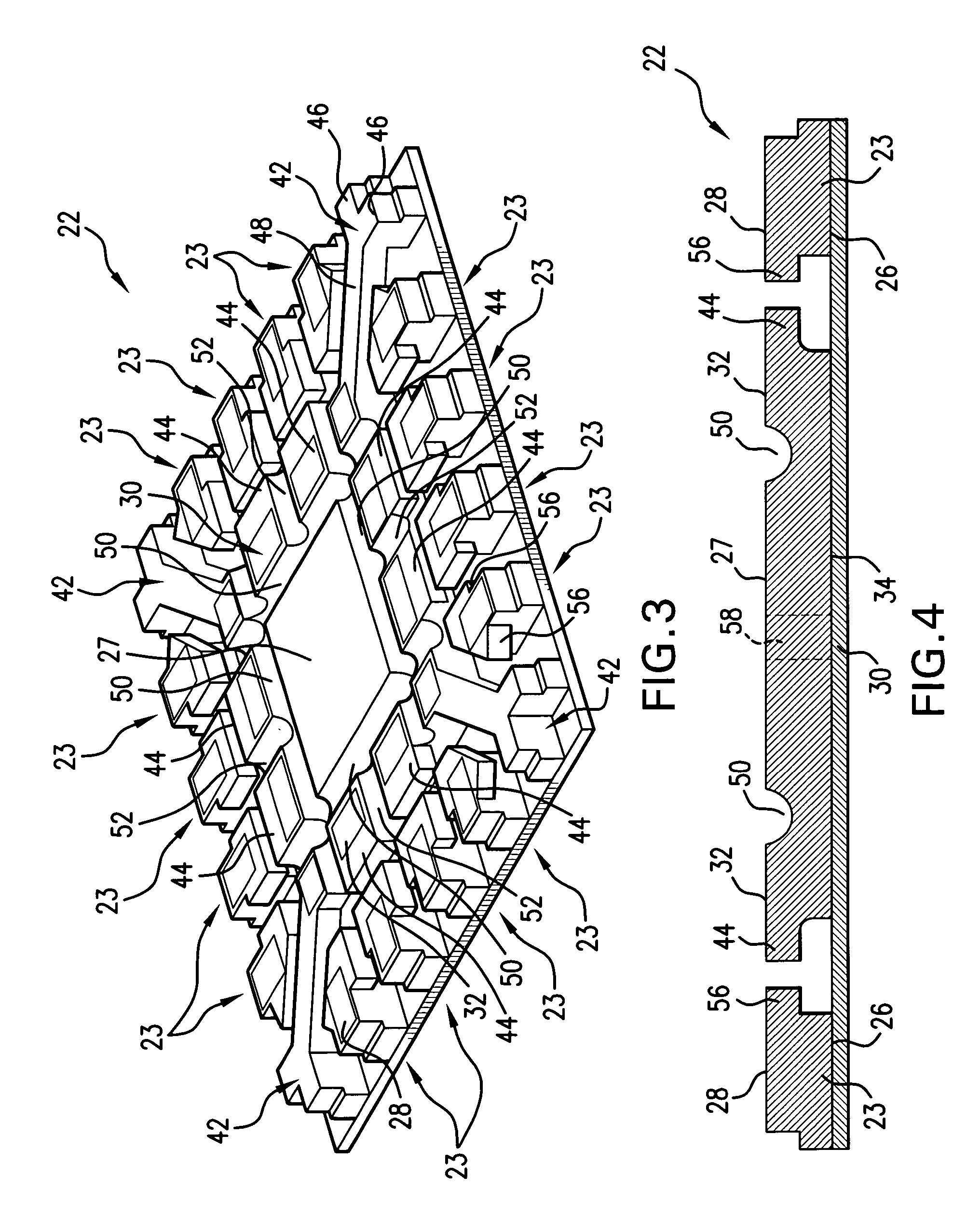
[0062]It is also contemplated that the number and location of the leads 23 may be modified as needed for a particular application. For example, FIG. 9 is a top perspective view of a lead frame 222 for a dual, no-lead, wirebonded semiconductor device package in accordance with the present invention, and FIG. 10 is a cross-sectional elevation view of the lead frame 222. The lead frame 222 of FIGS. 9 and 10 is substantially similar to the lead frame 22 shown in FIGS. 1-6, except that the lead frame 222 includes leads 23 disposed on two sides of the die pad 30 rather than on all four sides, as in the lead frame 22. Also unlike the die pad 30 in lead frame 22, the die pad 30 in lead frame 222 includes channels 50, 52 and tabs 44 on only two sides of the die pad 30 rather than four, and the tie bars 42 extend from the sides of the die pad 30 rather than the corners. Like the lead frame 22, the lead frame 222 includes a roughened surface 27 and channels 50 and 52 disposed in the die pad 30...


PUM


Abstract

A semiconductor device package comprising a semiconductor device and an electrically conductive lead frame at least partially covered by a molding compound. The electrically conductive lead frame includes a plurality of leads disposed proximate a perimeter of the package and a die pad disposed in a central region formed by the plurality of leads. The die pad includes a first die pad surface disposed at the first package face, and a second die pad surface opposite the first die pad surface. The semiconductor device is attached to a central region of the second die pad surface, and a portion of the second die pad surface extending outward from the die is roughened to improve adhesion of the die pad to the molding compound. In other aspects, grooves are disposed in the first and / or second die pad surfaces to further promote adhesion of the die pad and to prevent moisture from permeating into the vicinity of the semiconductor chip. The die pad may further include tie bars extending therefrom, and at least one lip at may extend from a side surface of the die pad to anchor the die pad in the molding compound. The die pad may also include apertures disposed therein for allowing the egress of moisture from the package.

Description

BACKGROUND OF THE INVENTION[0001]1. Field of the Invention[0002]This invention relates to semiconductor device packages. More particularly, this invention relates to semiconductor packages having die pads.[0003]2. Description of the Related Art[0004]Semiconductor device packages provide environmental protection to integrated circuit devices (dies). Such packages typically include at least one semiconductor device (die) having its input / output (I / O) pads electrically connected to a lead frame type substrate or an interposer type substrate, with a molding compound coating the die and at least a portion of the substrate. Typically, the I / O pads on the die are electrically connected to bond sites on the substrate using either a wire bonding, tape bonding, or flip-chip bonding method. The lead frame or interposer substrate transmits electrical signals between the I / O pads and an electrical circuit external to the package.[0005]In semiconductor device packages having a lead frame type sub...

Claims


Application Information

Patent Timeline
Patent Type & Authority Patents(United States)
IPC IPC(8): H01L23/495H01L29/06
CPCH01L21/561H01L21/568H01L23/3107H01L23/49503H01L23/49548H01L24/49H01L24/97H01L24/29H01L24/86H01L2224/2919H01L2224/32245H01L2224/45124H01L2224/45144H01L2224/48091H01L2224/48227H01L2224/48247H01L2224/48257H01L2224/48465H01L2224/4911H01L2224/49171H01L2224/73265H01L2224/83001H01L2224/83101H01L2224/85001H01L2224/85205H01L2224/85439H01L2224/85444H01L2224/85455H01L2224/85464H01L2224/92H01L2224/92247H01L2224/97H01L2924/01002H01L2924/01013H01L2924/01015H01L2924/01028H01L2924/01029H01L2924/01033H01L2924/01046H01L2924/01047H01L2924/01078H01L2924/01079H01L2924/01082H01L2924/01088H01L2924/014H01L2924/14H01L2924/18301H01L2924/19107H01L2924/00014H01L2224/82H01L2224/85H01L2224/83H01L2224/86H01L2924/0665H01L24/48H01L2924/01006H01L2924/00H01L2224/45139H01L2924/00012H01L2924/3512H01L2924/181H01L2224/48639H01L2224/48644H01L2224/48655H01L2224/48664H01L2224/48739H01L2224/48744H01L2224/48755H01L2224/48764H01L2224/05599H01L24/73H01L24/45H01L2924/00011H01L2224/50H01L2224/49433H01L2224/2612H01L2224/45015H01L2924/207H01L2924/01005H01L23/495H01L23/34H01L23/52H01L23/10
Inventor ISLAM, SHAFIDULSAN ANTONIO, ROMARICO SANTOSSUBAGIO, ANANG
Owner ADVANCED INTERCONNECT TECH LTD
Why Eureka
Try Eureka