Semiconductor device and its manufacturing method

a technology of semiconductor devices and manufacturing methods, applied in the direction of semiconductor devices, electrical equipment, transistors, etc., can solve the problems of easy production of fine scratches, and achieve the effects of low reliability, small thickness, and high reliability

Inactive Publication Date: 2007-09-04
RENESAS ELECTRONICS CORP
View PDF10 Cites 37 Cited by
  • Summary
  • Abstract
  • Description
  • Claims
  • Application Information

AI Technical Summary

Benefits of technology

[0010]However, in the case of prior art 1, the adhesive sheet is broken through by the needle pin to directly upheave the semiconductor chip and therefore, a fine scratch is easily produced on a nonfunctional surface (an opposite surface of a terminal surface) of the semiconductor chip in contact with the adhesive sheet due to an impression of the needle-shaped upthrow pin.
[0038]Further, a semiconductor chip applied to a stack-type semiconductor device has a very small thickness of 100 μm or less. Therefore, if applying a semiconductor chip manufactured by a conventional method, a crack occurs when actually mounting it and thus, the reliability is low. However, if using a semiconductor chip manufactured by removal using an ultrasonic wave, it is possible to provide a semiconductor device having high reliability because the number of cracks is very small.

Problems solved by technology

However, in the case of prior art 1, the adhesive sheet is broken through by the needle pin to directly upheave the semiconductor chip and therefore, a fine scratch is easily produced on a nonfunctional surface (an opposite surface of a terminal surface) of the semiconductor chip in contact with the adhesive sheet due to an impression of the needle-shaped upthrow pin.

Method used


Image

  • Semiconductor device and its manufacturing method
  • Semiconductor device and its manufacturing method
  • Semiconductor device and its manufacturing method

Examples


embodiment 1

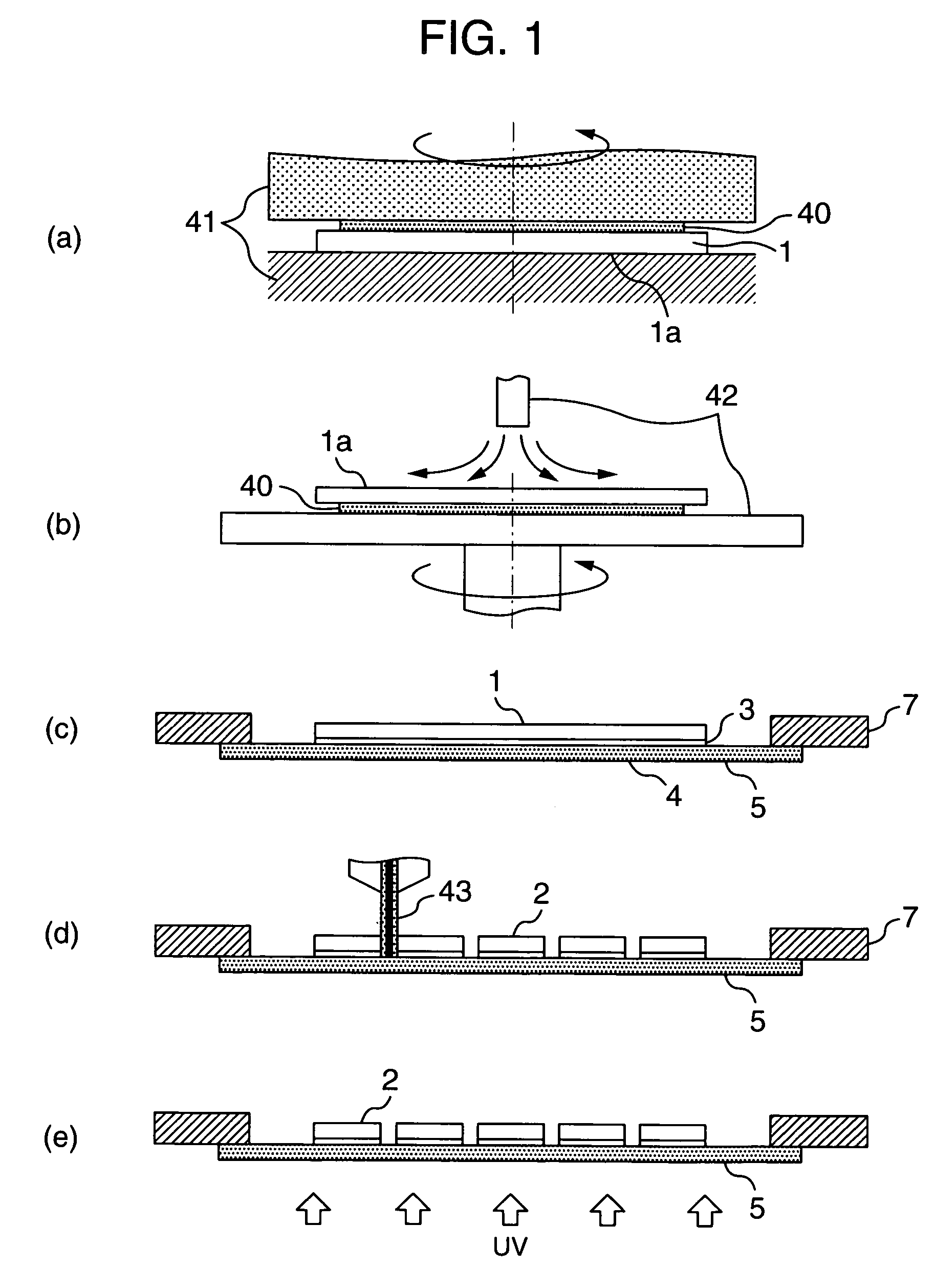
[0087]FIGS. 3(a) and 3(b) are sectional views showing an example of the upthrow operation of the chip separating unit of this embodiment 1 in order of the steps.

[0088]FIG. 4 is an enlarged sectional view showing an example of a state of an adhesive agent layer at the time of upthrowing by the chip separating unit of this embodiment 1.

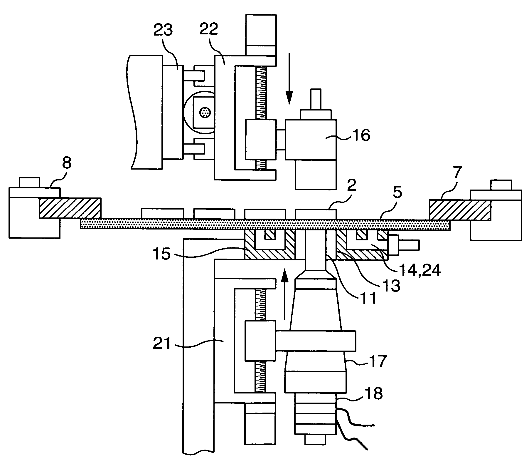
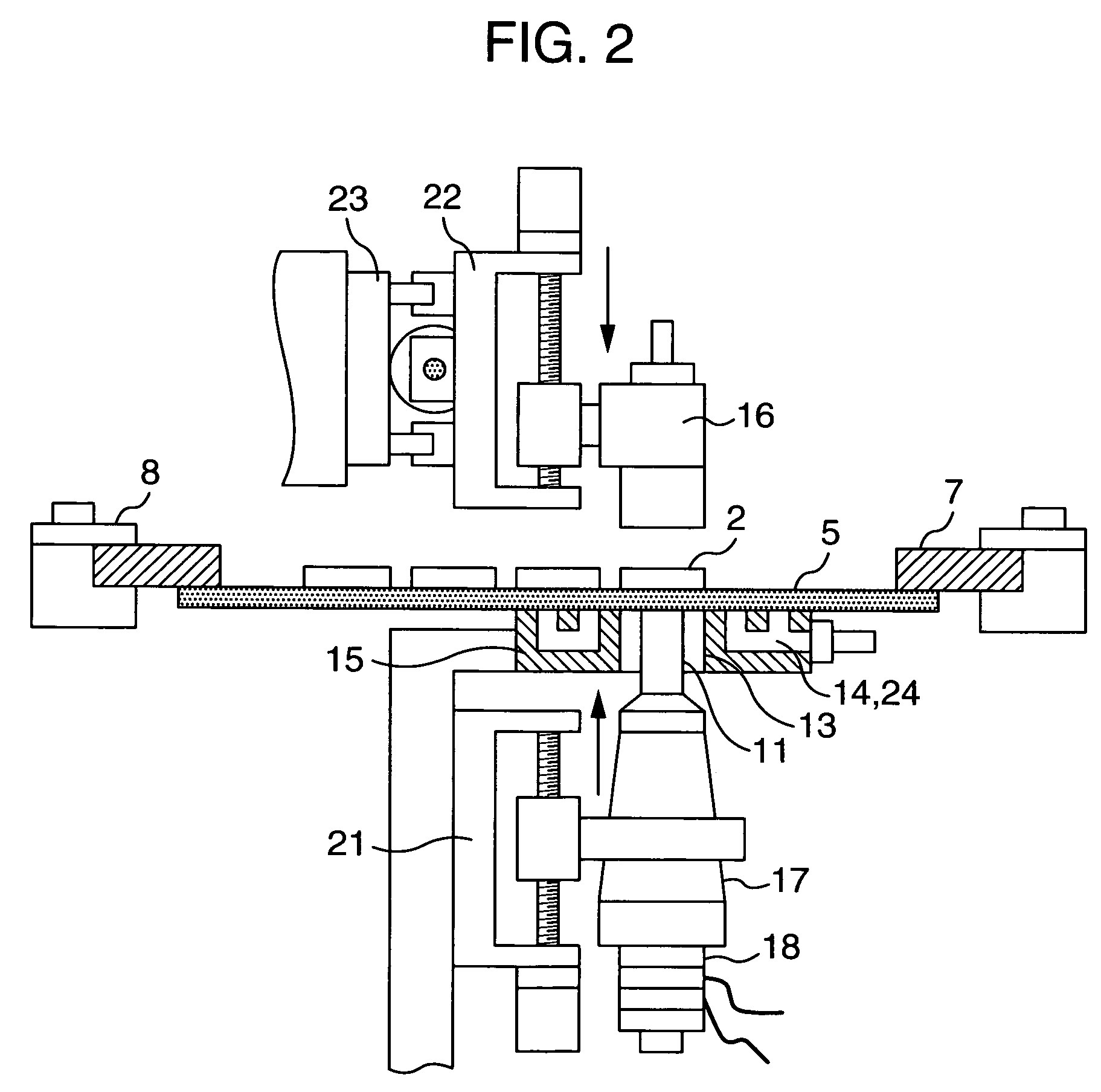
[0089]The chip separating unit of this embodiment 1 has a pickup stage 8 for supporting the adhesive sheet 5 to which the semiconductor chip 2 having been subjected to a dicing step is attached and the frame 7 to perform horizontal movement and positioning operation, a vacuuming stage 15 located under the pickup stage 8 to vacuum the back of the adhesive sheet 5, an upthrow jig 11 which is a jig for upthrowing the adhesive sheet 5 and semiconductor chip 2 and which is vertically movably set to an upthrow hole 13 at the center of the vacuuming stage, an ultrasonic vibrator 17 having a built-in piezoelectric device 18 arranged under the upthrow jig 11, an...

embodiment 3

[0145]FIG. 13 is a sectional view showing a chip separating unit used for a fabrication method of a semiconductor device of embodiment 3 of the present invention.

[0146]In the case of the chip separating unit of embodiment 1, the upthrow jig 11 is set to the ultrasonic wave oscillator 17 having built-in piezoelectric device 18 to use the upthrow jig 11 so that the aperture dimension and shape of the jig 11 can be changed or the frequency and amplitude of ultrasonic vibration can be changed in accordance with the size of the semiconductor chip 2 to be separated. However, it is also allowed to use a device for separating the semiconductor chip 2 by the single piezoelectric device 18 not through the upthrow jig 11.

[0147]The chip separating unit of embodiment 3 separates a chip in accordance with the same operation procedure as embodiment 1. A semiconductor chip 2 to be separated is upheaved by the tip end of a piezoelectric device 18 through an adhesive sheet 5 by vacuuming the back of ...

embodiment 4

[0148]FIG. 14 is a sectional view showing a chip separating unit used for a fabrication method of a semiconductor device of

[0149]In the case of the chip separating unit of embodiment 1, the semiconductor chip 2 attached to the adhesive sheet 5 is separated by raising the upthrow jig 11 from the backside of the sheet. However, it is also allowed to separate the semiconductor chip 2 by a device configuration in which all constituting devices are vertically reversed.

[0150]A chip separating unit of embodiment 4 has a pickup stage 8 for supporting an adhesive sheet 5 to which a semiconductor chip 2 having experienced a dicing step is attached and a frame 7 and performing horizontal movement and positioning, a vacuuming stage 15 located above the pickup stage 8 to vacuum the back of the adhesive sheet 5, an upthrow jig 11 located so as to be able to raise or lower a upthrow hole 13 at the center of the vacuuming stage to upthrow the adhesive sheet 5 and semiconductor chip 2, an ultrasonic...


PUM


Abstract

To improve the reliability and yield of a thin-type semiconductor device as used for a stack-type flash memory, the semiconductor device is manufactured by upheaving each of semiconductor chips (semiconductor devices) obtained by dicing a semiconductor wafer on an adhesive sheet from a backside via the adhesive sheet using an upthrow jig to which ultrasonic vibration is applied so as not to break through the adhesive sheet, and by picking up each semiconductor chip.

Description

BACKGROUND OF THE INVENTION[0001]The present invention relates to semiconductor device manufacturing technology.[0002]A semiconductor device manufacturing process includes a first step of simultaneously forming a plurality of semiconductor chips on a semiconductor wafer, a second step of attaching an adhesive sheet to the semiconductor wafer, a third step of dicing (cutting) the wafer and a part of the adhesive sheet so that the dies (the semiconductor chips) are not separated, and a fourth step of removing and picking up the cut-diced semiconductor chips from the adhesive sheet.[0003]As a prior art in the fourth step, there are known JP-A-02-230754 (prior arts 1 and 2), JP-A-05-109869 (prior art 3), JP-A-06-295930 (prior art 4), and JP-A-07-106363 (prior art 5).[0004]Prior art 1 discloses a technique in which a needle pin is inserted from a backside of an adhesive sheet to be removed, so as to break through the adhesive sheet by the inserting force and further, the pin directly uph...

Claims


Application Information

Patent Timeline
Patent Type & Authority Patents(United States)
IPC IPC(8): H01L21/00H01L21/68
CPCH01L21/67132H01L21/6836H01L21/6835H01L21/67092H01L2221/68327H01L2221/68322H01L21/68H01L21/78
Inventor HONMA, HIROSHIOOROKU, NORIYUKIODASHIMA, HITOSHIMITA, TORUMIYAZAKI, CHUICHIWADA, TAKASHI
Owner RENESAS ELECTRONICS CORP
Why Eureka
Try Eureka