Ferroelectric memory

a technology of ferroelectric memory and magnetic field, applied in the field of ferroelectric memory, can solve the problems of long read access time, drop in read margin, and difficult to precisely set the effective capacitance of the reference memory cell, and achieve the effect of easy generation and maximization of read margins of data

Inactive Publication Date: 2007-09-04
FUJITSU SEMICON LTD
View PDF7 Cites 14 Cited by
  • Summary
  • Abstract
  • Description
  • Claims
  • Application Information

AI Technical Summary

Benefits of technology

[0032]An object of the invention is to read data reliably from the memory cells even in case the residual dielectric polarization value of the ferroelectric capacitor is so low that the voltage change in the bit lines is small. Specifically, the object is to maximize the read margins of the data for individual logic values.
[0033]Another object of the invention is to retain the read margins of the data, even in case the ferroelectric capacitor is deteriorated, thereby to increase the rewrite number of the data.
[0034]Still another object of the invention is to shorten the read cycle time of the ferroelectric memory.

Problems solved by technology

In the read operation, therefore, the plate line drive scheme accompanied by a large CR delay has a defect that the read access time becomes long.
However, the effective capacitance of the reference memory cell is hard to set precisely to (C0+C1) / 2.
In case, however, an access is made in the next read operation to another memory cell MC which has not restored the residual dielectric polarization value Q, the reference memory cell has restored the residual dielectric polarization value Q. Therefore, the read margin has dropped, and the data may be unable to be correctly read.
In this ferroelectric memory, however, the operation of the sense amplifier cannot be started until the reference voltage is generated from the ferroelectric capacitor.
As a result, the access time is delayed.

Method used


Image

  • Ferroelectric memory
  • Ferroelectric memory
  • Ferroelectric memory

Examples


Embodiment Construction

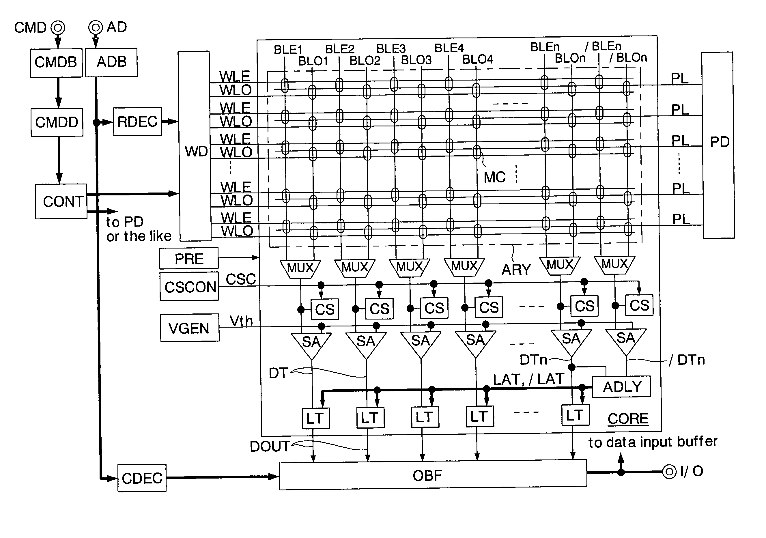
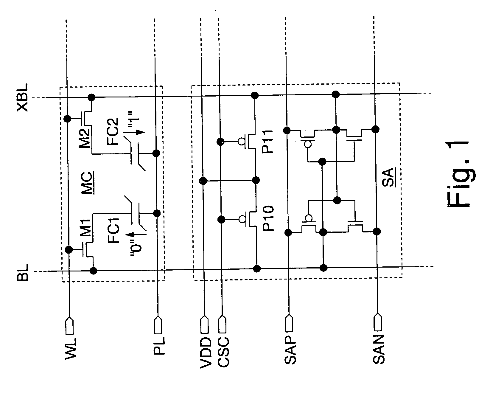
[0065]The embodiments of the invention will be described with reference to the accompanying drawings. Double circles in the drawings designate external terminals. Signal lines, which are indicated by bold lines in the drawings, are composed of a plurality of lines. Some of the blocks, which are connected with the bold lines, are composed of a plurality of circuits.

[0066]FIG. 5 shows an embodiment of the ferroelectric memory of the invention.

[0067]A ferroelectric memory chip is formed on a silicon substrate by using a CMOS process. This ferroelectric memory is used as a work memory of a hand-held terminal of a mobile phone, for example. The ferroelectric memory includes a command buffer CMDB, a command decoder CMDD, a control circuit CONT, an address buffer ADB, a row decoder RDEC, a column decoder CDEC, a word driver WD, a precharge circuit PRE, a current source control circuit CSCON, a threshold voltage generator VGEN, a memory core CORE, a plate driver PD and a data output buffer ...


PUM


Abstract

For a predetermined period from the start of a read operation, an electric current is fed to bit lines connected with memory cells so that ferroelectric capacitors of the memory cells are charged. The voltage change of the bit lines are different according to the logic values of data stored in the ferroelectric capacitors. Therefore, the logic value stored in the memory cells can be detected as a time difference. Even if the voltage change of the bit lines is small, the time difference can be reliably generated. Even in case the residual dielectric polarization value of the ferroelectric capacitor is low, therefore, the data can be reliably read from the memory cells. In short, the read margin of data can be better improved than in the case where the logic value of data is detected with a voltage difference.

Description

CROSS REFERENCE TO RELATED APPLICATION[0001]This application is a continuation application of International Application PCT / JP03 / 06601, filed on May 27, 2003, and designating the U.S.BACKGROUND OF THE INVENTION[0002]1. Field of the Invention[0003]The present invention relates to a ferroelectric memory having capacitors composed of ferroelectric films.[0004]2. Description of the Related Art[0005]As the semiconductor memory device having the advantages of all of a DRAM, a flash-memory, and an EEPROM, there has been developed a ferroelectric memory, which has memory cells provided with ferroelectric capacitors. The ferroelectric memory is enabled to hold data even if not fed with a power supply, by operating the ferroelectric capacitors made of an insulating material as a ferroelectric substance, as a variable capacitor and by utilizing the fact that a residual dielectric polarization is left even if the applied voltage to the ferroelectric capacitors is zero. The ferroelectric capacit...

Claims


Application Information

Patent Timeline
Patent Type & Authority Patents(United States)
IPC IPC(8): G11C11/22G11C29/02
CPCG11C11/22G11C29/02G11C29/023G11C29/028
Inventor CHANDLER, TREVISSHEIKHOLESLAMI, ALIMASUI, SHOICHI
Owner FUJITSU SEMICON LTD
Why Eureka
Try Eureka