Post-polish treatment for inhibiting copper corrosion

a post-polish treatment and copper technology, applied in the field of methods for treating copper structures, can solve the problems of increasing contact resistance and adhesion problems, interconnect leakage, and reducing the amount of metrology after cmp, so as to facilitate inspection and measurement, and facilitate sometimes lengthy metrology operations.

Active Publication Date: 2007-09-11
TEXAS INSTR INC
View PDF14 Cites 9 Cited by
  • Summary
  • Abstract
  • Description
  • Claims
  • Application Information

AI Technical Summary

Benefits of technology

[0006]The following presents a simplified summary in order to provide a basic understanding of one or more aspects of the invention. This summary is not an extensive overview of the invention, and is neither intended to identify key or critical elements of the invention, nor to delineate the scope thereof. The primary purpose of the summary is to present some concepts of the invention in a simplified form as a prelude to the more detailed description that is presented later. The invention relates to methods for treating copper structures to prevent or inhibit corrosion during fabrication processing of semiconductor devices, which may be advantageously employed to widen the process window for metrology operations following planarization steps in forming back-end metalization structures.
[0007]One aspect of the invention provides a method of protecting copper structures from corrosion in the fabrication of semiconductor devices. The method comprises providing a copper structure with an exposed first surface in a semiconductor device, forming a semiconductor or semiconductor-copper alloy corrosion protection layer on the exposed first surface of the copper structure, performing a metrology operation after forming the corrosion protection layer, and forming an etch-stop layer, such as silicon carbide or silicon nitride, over the corrosion protection layer after performing the metrology operation. The provision of the corrosion protection layer facilitates sometimes lengthy metrology operations in which the device wafer may be subjected to humidity or other corrosive environments, where the semiconductor or semiconductor-copper alloy provides a generally conductive surface over the exposed first surface of the copper structures that facilitates inspection and measurement of various features or qualitative aspects of the device while protecting the upper copper surfaces from corrosion.
[0010]Yet another aspect of the invention provides a method of protecting copper structures from corrosion in the fabrication of semiconductor devices. The method comprises providing a copper structure with an exposed first surface in a semiconductor device, exposing the first surface of the copper structure to a plasma-free silane gas treatment for a short time, such as about 40 seconds or less, to form a corrosion protection layer, for example, a semiconductor or a semiconductor-copper alloy, on the exposed first surface of the copper structure, and forming an etch-stop layer over the corrosion protection layer. The method may further comprise performing a metrology operation after the plasma-free silane gas treatment and before forming the etch-stop layer.

Problems solved by technology

Often, such metrology takes 8-12 hours, wherein reducing the amount of metrology after CMP risks missing an early detection of defects in the metalization structures.
However, the planarization exposes the upper surfaces of the copper-filled trenches and vias to moisture and other corrosive ambient conditions, particularly where the planarized wafers are transferred from instrument to instrument to perform the desired metrology operations.
Such corrosive ambient conditions cause oxidation and other degradation of the copper, leading to increased contact resistance and adhesion problems in subsequent fabrication processing.
Corrosion of copper interconnect structures is detrimental to interconnect isolation integrity, and can lead to interconnect leakage between copper structures in a single metalization level, as well as premature dielectric breakdown (e.g., reduced breakdown voltage withstanding capacity).
The corrosion tends to migrate outward from the edges of the structure, thereby reducing the isolation distance between adjacent conductive features, by which the likelihood of detrimental intra-level dielectric breakdown is increased.
However, BTA coatings tend to evaporate and the corrosion protection typically only lasts for 3-6 hours.
This process time window for making measurements of the planarized wafer is insufficient to allow the full range of metrology operations desired to effectively sort out defective wafers, where a longer process window of up to 12 hours or more is desirable.
Thus, while forming the etch-stop layer prior to metrology may inhibit unwanted copper corrosion, this approach inhibits the ability to obtain proper metrology measurements.

Method used


Image

  • Post-polish treatment for inhibiting copper corrosion
  • Post-polish treatment for inhibiting copper corrosion
  • Post-polish treatment for inhibiting copper corrosion

Examples


Embodiment Construction

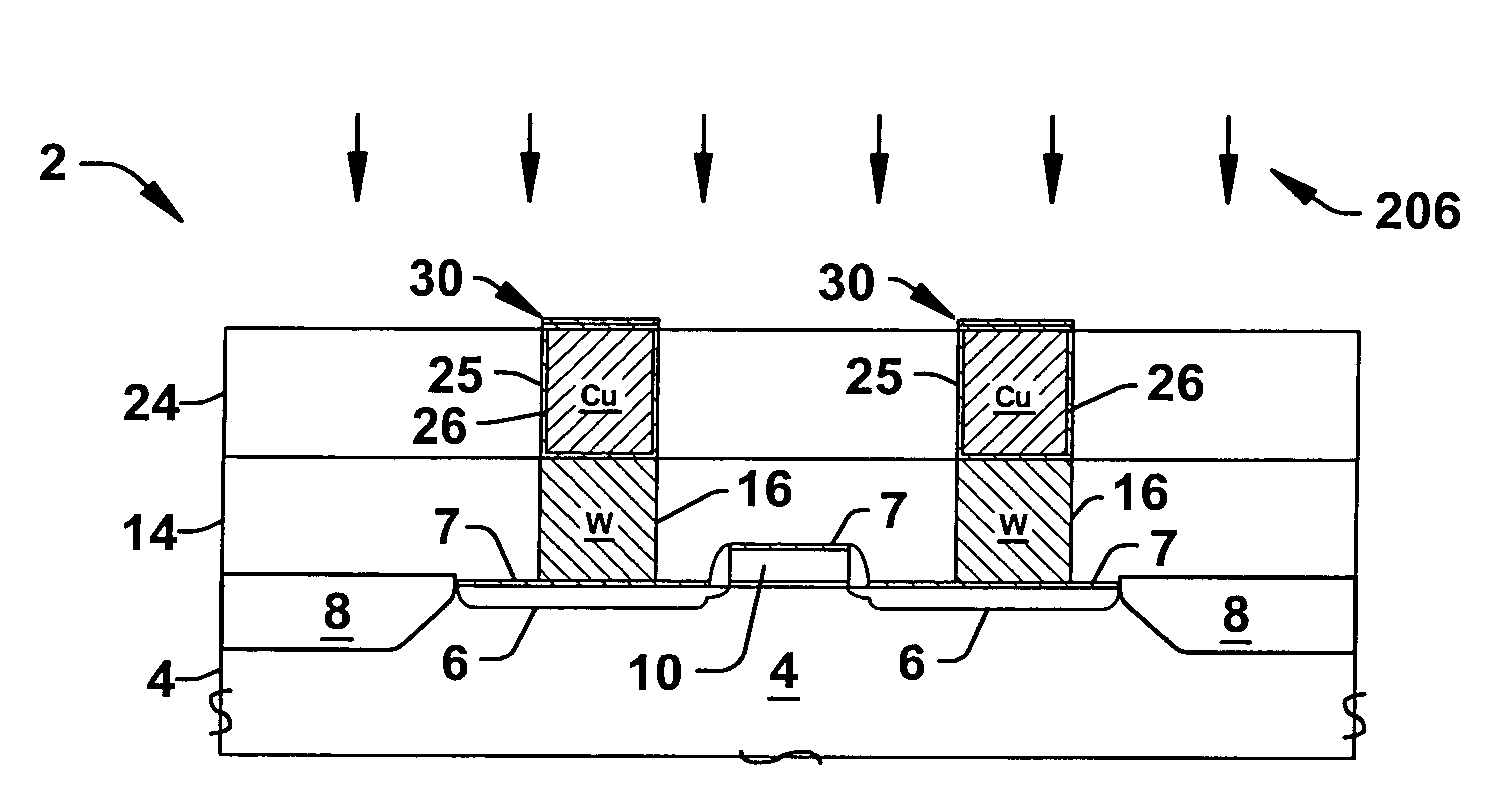
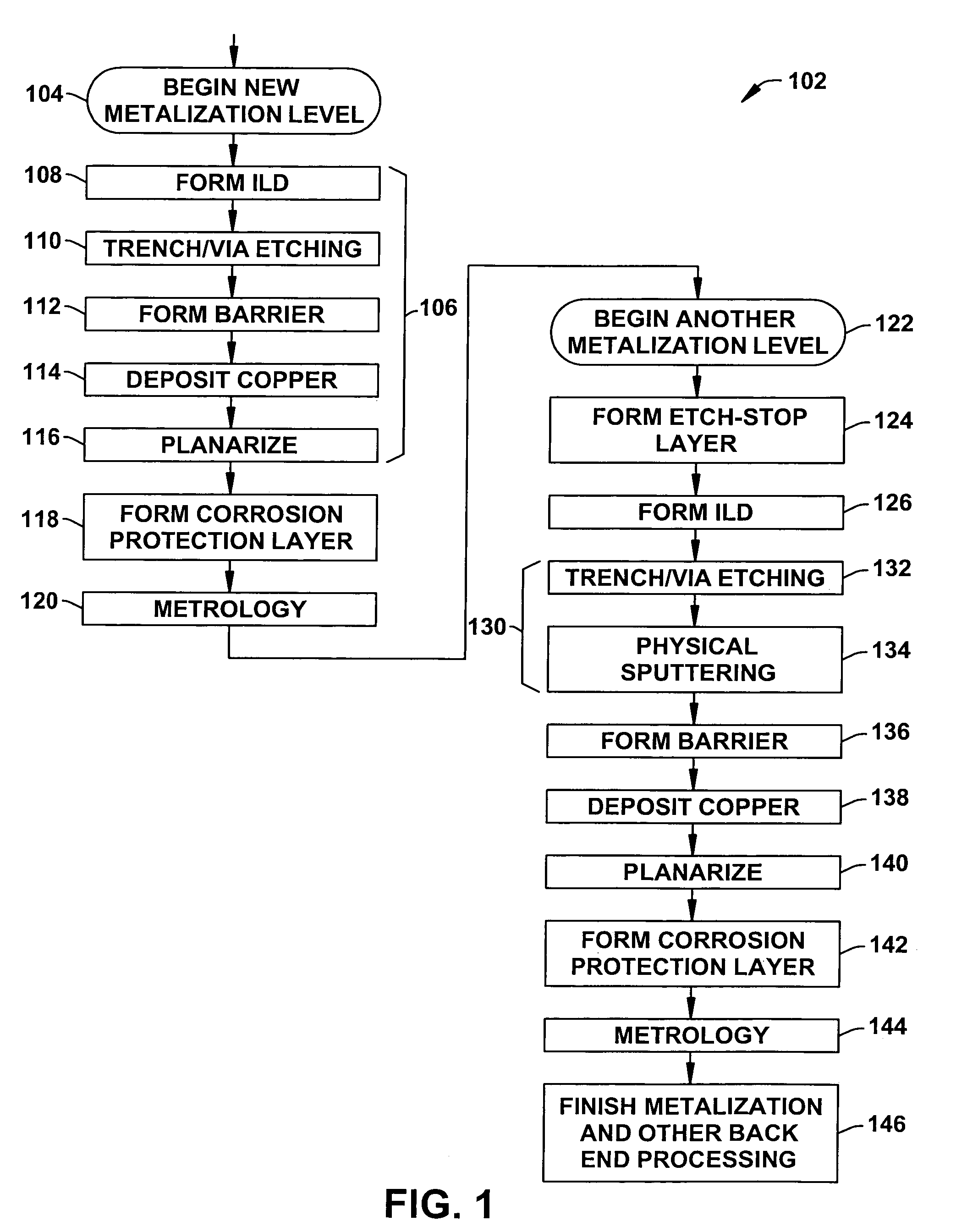
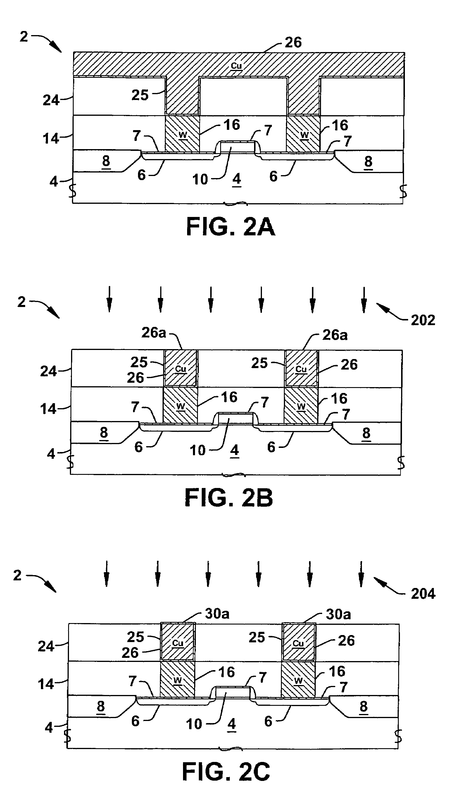
[0014]The present invention will now be described with reference to the attached drawings, in which like reference numerals are used to refer to like elements throughout, wherein the illustrated structures are not necessarily drawn to scale. The invention relates to semiconductor device interconnect system fabrication processing and methods for protecting copper against corrosion, which may be employed at any point in a fabrication process flow. The invention is hereinafter illustrated and described in the construction of damascene type metalization interconnect structures, wherein protection is provided to prevent corrosion of copper surfaces exposed after planarization. However, the invention is not limited to the exemplary implementations illustrated and described hereinafter. In particular, the various aspects of the invention may be employed in association with processing of any type of copper structures, and may be used for protecting any surface or surfaces thereof from corro...


PUM


Abstract

Methods (102) are presented for protecting copper structures (26) from corrosion in the fabrication of semiconductor devices (2), wherein a thin semiconductor or copper-semiconductor alloy corrosion protection layer (30) is formed on an exposed surface (26a) of a copper structure (26) prior to performance of metrology operations (206), so as to inhibit corrosion of the copper structure (26). All or a portion of the corrosion protection layer (30) is then removed (214) in forming an opening in an overlying dielectric (44) in a subsequent interconnect layer.

Description

FIELD OF INVENTION[0001]The present invention relates generally to semiconductor devices and more particularly to methods for treating copper structures to prevent or inhibit corrosion in the fabrication of semiconductor devices.BACKGROUND OF THE INVENTION[0002]In the manufacture of semiconductor products such as integrated circuits, individual electrical components are formed on or in a semiconductor substrate, and are thereafter interconnected to form electrical circuits. Interconnection of these components within a semiconductor device is typically accomplished by forming a multi-level interconnect network structure in layers formed over the electrical components, sometimes referred to as metalization, by which the device active elements are connected to other devices to create the desired circuits. Individual wiring layers within the multi-level network are formed by depositing an insulating or dielectric layer over the discrete devices or over a previous interconnect layer, and...

Claims


Application Information

Patent Timeline
Patent Type & Authority Patents(United States)
IPC IPC(8): H01L21/44
CPCH01L21/7684H01L21/76886
Inventor RAMAPPA, DEEPAK A.EISSA, MONABORST, CHRISTOPHER LYLETSUI, TING Y.
Owner TEXAS INSTR INC
Why Eureka
Try Eureka