Memory module and impedance calibration method of semiconductor memory device

a memory module and impedance calibration technology, applied in the field of memory modules, can solve the problems of resistors mounted on the memory modules, inefficiency in cost and space, and complicated wiring, and achieve the effects of calibrating impedance characteristics, and calibrating impedance characteristics of the semiconductor memory devi

Active Publication Date: 2007-09-11
SAMSUNG ELECTRONICS CO LTD
View PDF6 Cites 51 Cited by
  • Summary
  • Abstract
  • Description
  • Claims
  • Application Information

AI Technical Summary

Problems solved by technology

However, if the memory module, including the semiconductor memory devices that calibrate an impedance calibration using a ZQ terminal, is configured as shown in FIG. 2, the number of the reference resistors mounted on the memory module is increased, which complicates the wiring and causes inefficiencies in cost and space.

Method used


Image

  • Memory module and impedance calibration method of semiconductor memory device
  • Memory module and impedance calibration method of semiconductor memory device
  • Memory module and impedance calibration method of semiconductor memory device

Examples


Embodiment Construction

[0041]The present disclosure will now be described more fully hereinafter with reference to the accompanying drawings, in which preferred embodiments of the disclosure are shown. This disclosure may, however, be embodied in different forms and should not be construed as limited to the embodiments set forth herein. Rather, these embodiments are provided so that this disclosure will be thorough and complete, and will fully convey the scope of the disclosure to those skilled in the pertinent art. Like reference numbers may refer to like elements throughout the specification.

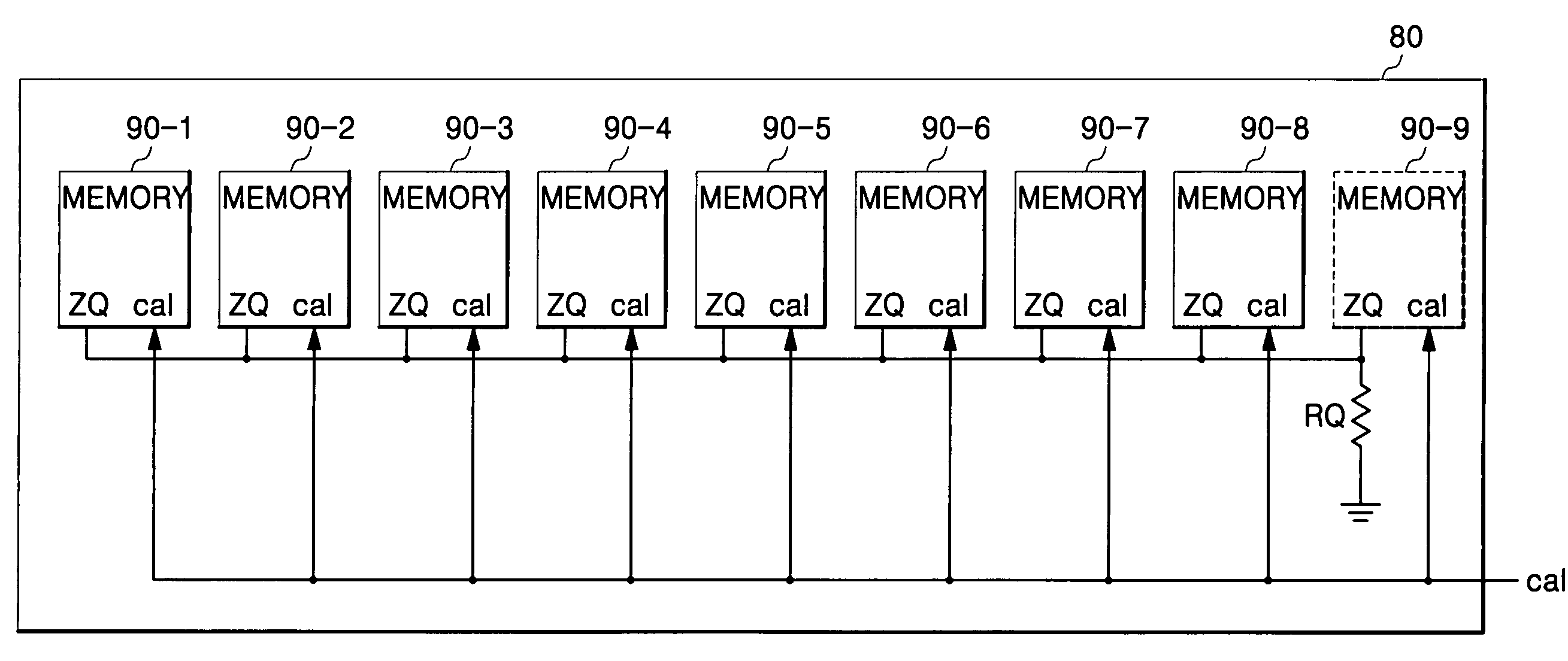
[0042]FIG. 3 is a block diagram illustrating a memory module according to an embodiment of the present disclosure. The memory module of FIG. 3 includes a plurality of semiconductor memory devices 90-1 to 90-9, and a single reference resistor RQ. The plurality of semiconductor memory devices 90-1 to 90-9 have separate ZQ terminals for calibrating impedance characteristics of semiconductor memory devices.

[0043]Functio...


PUM


Abstract

Disclosed is a memory module and a method of calibrating an impedance of a semiconductor memory device of the memory module, where the memory module includes semiconductor memory devices each having a separate terminal for calibrating impedance characteristics, and a reference resistor commonly connected to the separate terminals, such that the number of reference resistors used in calibration of impedance characteristics of an off-chip driver or an on-die termination circuit of the semiconductor memory device is reduced.

Description

BACKGROUND OF THE INVENTION[0001]1. Field of the Invention[0002]The present disclosure relates to memory modules and, more particularly, to a memory module and an impedance calibration method of a semiconductor memory device.[0003]2. Description of the Related Art[0004]Semiconductor integrated circuit (IC) devices such as microcontrollers and memory devices receive and transmit data from / to other semiconductor IC devices through a transmission line. For this reason, most semiconductor IC circuit devices include an off-chip driver (OCD) for outputting signals to an external portion from the semiconductor IC device, and an on-die termination circuit (ODT) for preventing a reflection of signals transmitted to the semiconductor IC device from an external portion. In this case, in order to secure signal integrity, it is required to calibrate impedance characteristics of the off-chip driver or the on-die termination circuit. As systems operate at increasingly higher speeds, the need for c...

Claims


Application Information

Patent Timeline
Patent Type & Authority Patents(United States)
IPC IPC(8): G11C5/06G11C5/00G11C7/00G11C7/10G11C29/38
CPCG11C5/04G11C29/028G11C29/38G11C29/50008G11C2207/2254G11C7/10
Inventor LEE, JUNG-BAE
Owner SAMSUNG ELECTRONICS CO LTD
Why Eureka
Try Eureka