Semiconductor device having triple-well structure

a technology of semiconductor devices and transistors, which is applied in the direction of semiconductor devices, transistors, electrical devices, etc., can solve the problems of increasing p-well resistance and the inability to reduce the area of memory cells, so as to increase the latch-up breakdown voltage, reduce the n-well resistance advantageously, and increase the p-well resistance

Active Publication Date: 2007-09-18
GK BRIDGE 1
View PDF3 Cites 6 Cited by
  • Summary
  • Abstract
  • Description
  • Claims
  • Application Information

AI Technical Summary

Benefits of technology

[0010]In view of the foregoing, it is therefore an object of the present invention to reduce N-well resistance in a semiconductor device having a triple-well structure and thereby increase latch-up breakdown voltage, while suppressing an increase in P-well resistance.
[0013]In the semiconductor device according to the present invention, the individual second well regions of the second conductivity type (e.g., N-well regions) are connected electrically to each other by the third well region of the second conductivity type (e.g., a Deep-N-well region) formed at a deeper position so that the N-well resistance is reduced advantageously. Accordingly, even when a surge current flows into, e.g., a specified one of the N-well regions, it becomes possible to prevent the localization of the surge current to the specified N-well region or to the device formed therein and thereby increase the latch-up breakdown voltage.
[0014]In the semiconductor device according to the present invention, at least a portion of the first well region of the first conductivity type (e.g., a P-well region) is electrically connected to the semiconductor substrate of the first conductivity type (e.g., a P-type substrate and, more specifically, the region of the P-type substrate in which the Deep-N-well region is not formed) in the triple-well structure without intervention of a contact. This suppresses an increase in P-well resistance. Since it is no more necessary to provide a contact area for providing the surface of the P-well with a substrate potential, the chip area can be reduced accordingly by the reduced contact area.
[0015]Since the present invention has thus provided the Deep-N-well which electrically connects the N-well regions to each other in such a manner as to leave the region in which the P-well and the P-type substrate are electrically connected to each other, the latch-up breakdown voltage can be increased by reducing the N-well resistance, while suppressing an increase in P-well resistance. The present invention has also connected to the P-well and the P-type substrate to each other so that the chip area is reduced advantageously by reducing the contact area for providing the surface of the P-well with the substrate potential.
[0016]As described above, the present invention relates to the semiconductor device comprising the MIS transistor having the triple-well structure and to the fabrication method therefor. When applied to an extremely small memory cell such as an SRAM, the present invention particularly achieves the effect of increasing the latch-up breakdown voltage by reducing the N-well resistance, while suppressing an increase in P-well resistance, and is therefore extremely useful.

Problems solved by technology

Although the problem of the increased N-well resistance can be solved when the memory cell of a semiconductor device composed of a MIS transistor, such as an SRAM, is provided with the conventional triple-well structure, the problem of increased P-well resistance occurs because the Deep-N-well that has been formed in the entire region under the P-well isolates the P-well from the P-type substrate.
To provide the P-well with a substrate potential, it becomes necessary to provide a contact area for providing the surface of the P-well with the substrate potential, which causes the problem that the area of the memory cell cannot be reduced.

Method used


Image

  • Semiconductor device having triple-well structure
  • Semiconductor device having triple-well structure
  • Semiconductor device having triple-well structure

Examples


embodiment 1

[0037]Referring to the drawings, a description will be given herein below to a semiconductor device according to a first embodiment of the present invention and to a fabrication method therefor by using the memory cell portion of an SRAM composed of MIS transistors.

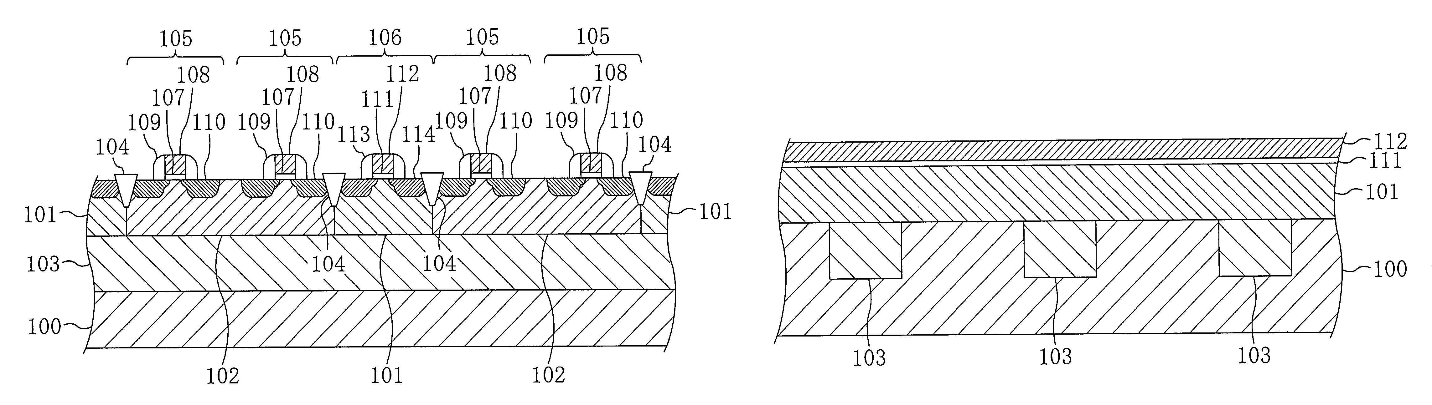
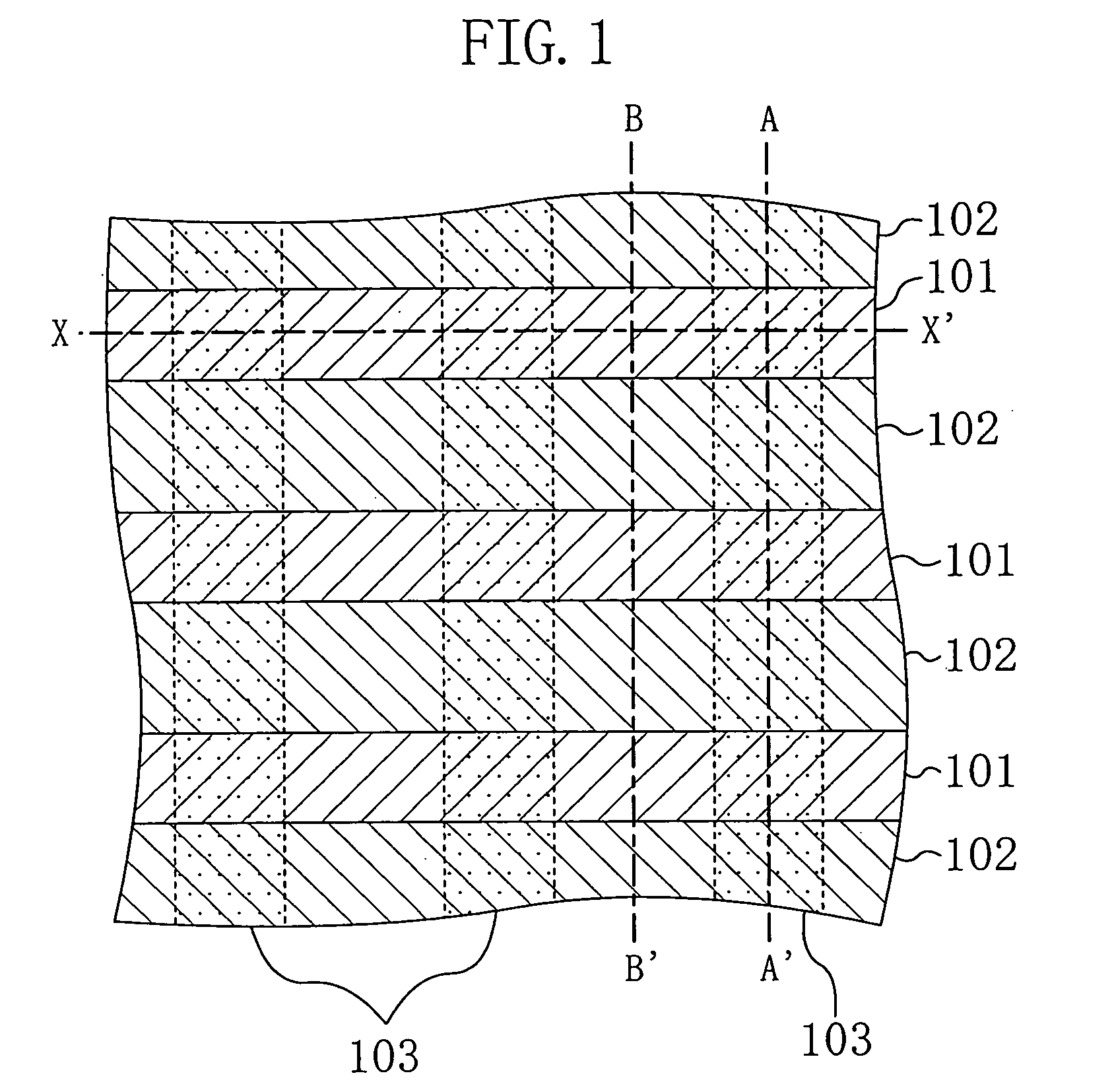
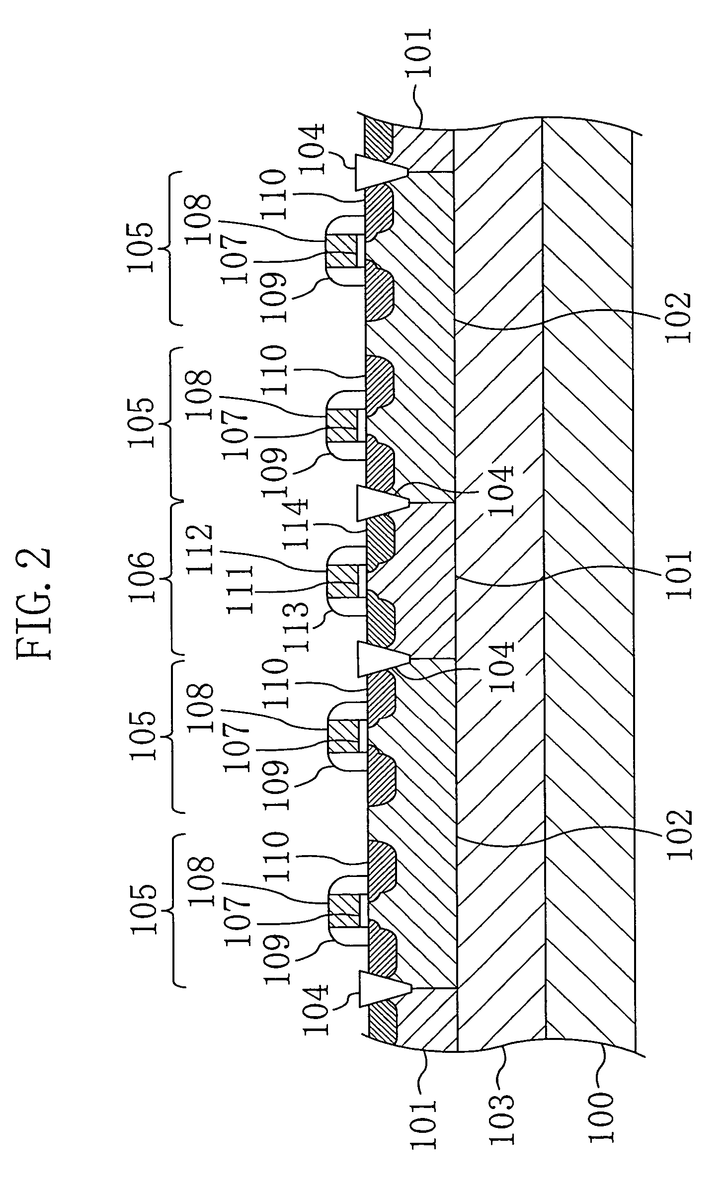
[0038]FIG. 1 is a plan view showing an example of the layout of the memory cell portion of the SRAM according to the present invention. FIG. 2 is a cross-sectional view taken along the line A-A′ of FIG. 1. FIG. 3 is a cross-sectional view taken along the line B-B′ of FIG. 1. FIG. 4 is a cross-sectional view taken along the line X-X′ of FIG. 1. In FIG. 1, the depiction of transistor structures formed on individual well regions is omitted.

[0039]As shown in FIGS. 1 to 4, a plurality of N-well regions 101 and a plurality of P-well regions 102 are formed to be alternately arranged, each extending from a surface of a P-type semiconductor substrate 100 toward the inside thereof. Between the N-well regions 101 and the P-well regi...

embodiment 2

[0057]Referring to the drawings, a description will be given herein below to a semiconductor device and a fabrication method therefor according to a second embodiment of the present invention by using the memory cell portion of an SRAM composed of MIS transistors with reference to the drawings.

[0058]FIG. 12 is a plan view showing an example of the layout of the memory cell portion of the SRAM according to the present embodiment. FIG. 13 is a cross-sectional view taken along the line E-E′ of FIG. 12. FIG. 14 is a cross-sectional view taken along the line F-F′ of FIG. 12. FIG. 15 is a cross-sectional view taken along the line Y-Y′ of FIG. 12.

[0059]In FIG. 12, the depiction of transistor structures formed on the individual well regions is omitted.

[0060]As shown in FIGS. 12 to 15, a plurality of N-well regions 201 and a plurality of P-well regions 202 are formed to be alternately arranged, each extending from a surface of a P-type semiconductor substrate 200 toward the inside thereof. B...


PUM


Abstract

A semiconductor device has a semiconductor substrate of a first conductivity type, a first well region of the first conductivity type which is formed to extend from the surface of the semiconductor substrate toward the inside thereof, a pair of second well regions of a second conductivity which are formed to extend from the surface of the semiconductor substrate toward the inside thereof in such as manner as to sandwich the first well region therebetween, and a third well region of the second conductivity type which is formed under each of the first well region and the pair of second well regions in the semiconductor substrate. The third well region electrically connects the pair of second well regions to each other. The first well region has at least a portion thereof connected to the region of the semiconductor substrate in which the third well region is not formed.

Description

BACKGROUND OF THE INVENTION[0001]The present invention relates to a semiconductor device comprising a MIS transistor having a triple-well structure and to a fabrication method therefor. More particularly, it aims at increasing latch-up breakdown voltage.[0002]As semiconductor devices have been increasingly miniaturized with recent advances in semiconductor fabrication technologies, the arrangement pitch of transistors has been reduced rapidly. As a result, the resistance of a well has increased prominently so that the lowering of latch-up breakdown voltage has presented a problem. Specifically, since an implantation angle (tilt angle) of about 7° is used in the ion implantation of an impurity for forming a well, an implant mask (resist) becomes a barrier in a well in the vicinity of the mask so that an amount of the implanted impurity is reduced and the impurity concentration is thereby lowered. The influence of the lowered concentration is negligible when the width of the well is l...

Claims


Application Information

Patent Timeline
Patent Type & Authority Patents(United States)
IPC IPC(8): H01L29/76H01L29/94H01L31/062H01L31/113H01L31/119H01L21/8238H01L21/8244H01L27/08H01L27/088H01L27/092H01L27/11
CPCH01L21/823892H01L27/0928
Inventor MISAKI, MAKOTOKURIMOTO, KAZUMI
Owner GK BRIDGE 1
Why Eureka
Try Eureka