Wordline voltage generating circuit including a voltage dividing circuit for reducing effects of parasitic capacitance

a voltage generation circuit and parasitic capacitance technology, applied in static storage, digital storage, instruments, etc., can solve the problems of parasitic capacitance, variable wordline voltage variation, and dividing voltage not keeping up with wordline voltage variations at high speed operation, so as to reduce parasitic capacitance

Active Publication Date: 2007-09-18
SAMSUNG ELECTRONICS CO LTD
View PDF10 Cites 19 Cited by
  • Summary
  • Abstract
  • Description
  • Claims
  • Application Information

AI Technical Summary

Benefits of technology

[0009]The present invention is directed to, among other things, a voltage dividing circuit capable of reducing the effect of parasitic capacitance.

Problems solved by technology

A volatile memory loses data if power is not supplied.
When the parasitic capacitance increases, the dividing voltage may not keep up with variations in the wordline voltage at high speed operation.
As a result, there is a likelihood that overshoot will occur in the wordline voltage.
Furthermore, there may be a ripple in the wordline voltage rather than there being a constant wordline voltage.

Method used


Image

  • Wordline voltage generating circuit including a voltage dividing circuit for reducing effects of parasitic capacitance
  • Wordline voltage generating circuit including a voltage dividing circuit for reducing effects of parasitic capacitance
  • Wordline voltage generating circuit including a voltage dividing circuit for reducing effects of parasitic capacitance

Examples


Embodiment Construction

[0021]Hereinafter, an exemplary embodiment of the present invention will be described in conjunction with the accompanying drawings.

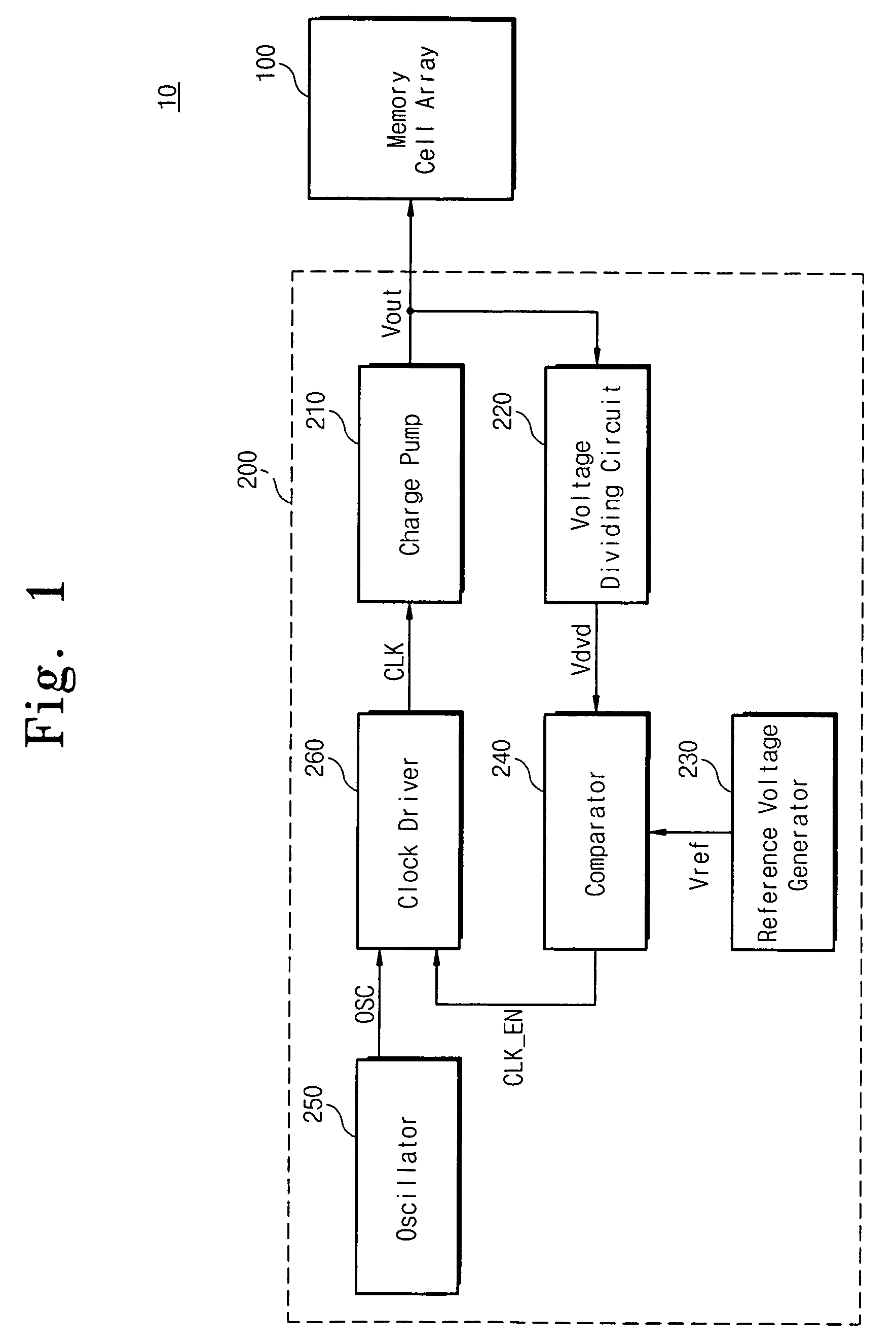
[0022]FIG. 1 is a block diagram showing a wordline voltage generating circuit according to a first embodiment of the present invention. As shown in FIG. 1, a flash memory device 10 includes a memory cell array 100 and a wordline voltage generating circuit 200. The wordline voltage generating circuit 200 provides a stable output voltage Vout with a small amount of overshoot and ripple.

[0023]The memory cell array 100 has a plurality of memory cells (not shown in the Figure) connected to a word line and a bit line. Such an array and the connections to the array are conventional. The wordline voltage generating circuit 200 selectively applies a wordline voltage to a selected memory cell during a write / read / erase operation.

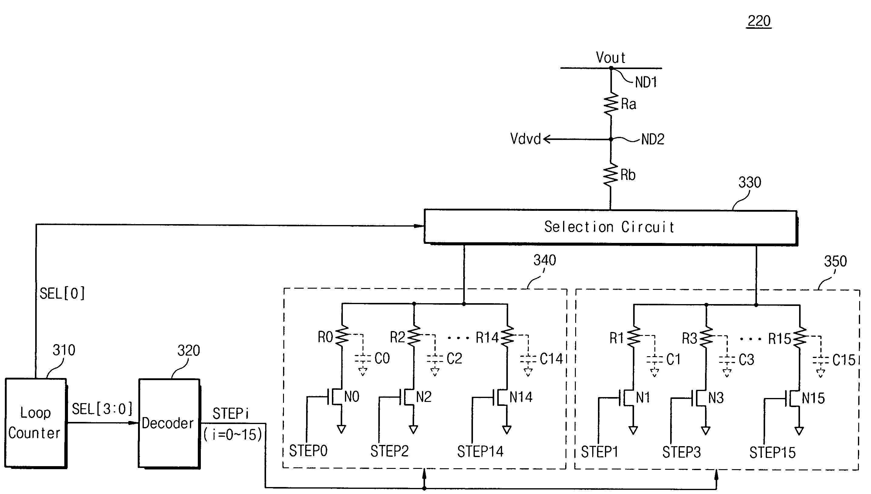
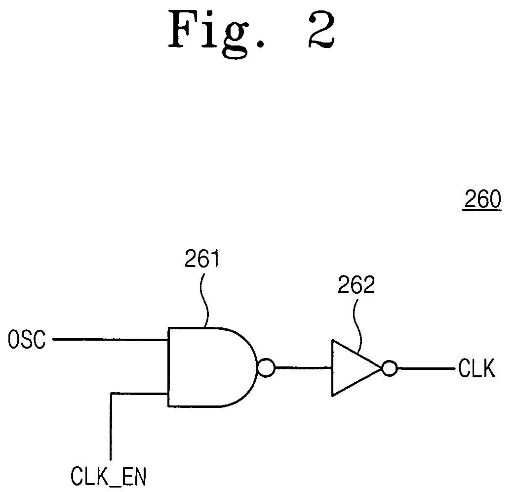
[0024]As shown in FIG. 1, the wordline voltage generating circuit 200 includes a charge pump 210, a voltage dividing circuit 220, a refer...


PUM


Abstract

Disclosed is a voltage dividing circuit reducing effects of a parasitic capacitance and a wordline voltage generating circuit including that. The voltage dividing circuit according to an aspect of the present invention includes a first resistor, a plurality of second resistors, and a selection means. The first resistor is connected between an output voltage node and a dividing voltage node. The plurality of second resistors are connectable between the dividing voltage node and a ground. The second resistors are sequentially selected in response to a step control signal and connected to ground. In order to reduce the sum of a parasitic capacitance existing in the second resistors, the resistors are arranged in groups, and the selection means connects only that group that contains a selected resistor to the dividing voltage node.

Description

CROSS-REFERENCE TO RELATED APPLICATIONS[0001]This application hereby claims priority under 35 U.S.C. § 119 to Korean Patent Application 2004-86304 filed on Oct. 27, 2004. The entire contents of Korean Patent Application 2004-86304 is hereby incorporated herein by reference.FIELD OF THE INVENTION[0002]The present invention relates to semiconductor memory devices, and more particularly to wordline voltage generating circuits.BACKGROUND OF THE INVENTION[0003]Semiconductor memory devices are generally classified into Random Access Memory (RAM) and Read Only Memory (ROM) devices. Semiconductor memory devices can also be classified as volatile or non volatile. A volatile memory loses data if power is not supplied. A nonvolatile memory keeps previously stored data even if power is not supplied.[0004]RAM devices include Dynamic RAM (DRAM) and Static RAM (SRAM), and ROM memories. ROM devices include Programmable ROM (PROM), Erasable PROM (EPROM), Electrically EPROM (EEPORM), and flash memori...

Claims


Application Information

Patent Timeline
Patent Type & Authority Patents(United States)
IPC IPC(8): G11C11/34G11C16/04G11C7/00
CPCG11C8/08G11C7/02G11C16/12G11C16/34
Inventor CHAE, DONG-HYUKBYEON, DAE-SEOK
Owner SAMSUNG ELECTRONICS CO LTD
Why Eureka
Try Eureka