Reactive barrier/seed preclean process for damascene process

a damascene and reactive barrier technology, applied in the field of electronic components, can solve the problems of copper oxide being detrimental to the integrated circuit device, copper out-diffusion into the dielectric layer, and argon being found to damage the insulation effect of the dielectri

Active Publication Date: 2007-09-25
NOVELLUS SYSTEMS
View PDF6 Cites 22 Cited by
  • Summary
  • Abstract
  • Description
  • Claims
  • Application Information

AI Technical Summary

Benefits of technology

[0026]In a further aspect of the invention the composition comprising the nitrogen containing material and oxygen containing material is gaseous and the composition compri...

Problems solved by technology

Copper oxide is detrimental to the integrated circuit (IC) device and must be removed before further processing.
The use of argon however, has a tendency to resputter copper onto the damascen...

Method used


Image

  • Reactive barrier/seed preclean process for damascene process

Examples


example

[0046]The following example shows the effect on the k-shift of a low-k dielectric material when using the method of the invention as compared to conventional prior art methods.

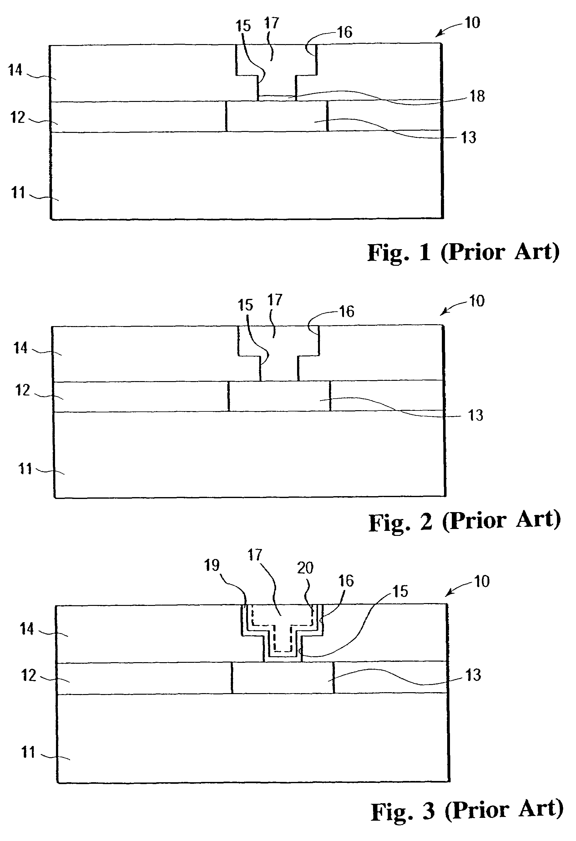
[0047]In the table below, the use of energized nitrogen gas and oxygen gas in combination is shown to clean a dual damascene interconnect as shown in FIG. 1 and is compared with the prior art methods using argon and argon / hydrogen. The dielectric material is silicon dioxide. All the treatments shown in the table were effective to remove the copper oxide layer but, as noted in the table, the method of the invention had a significantly lower k-shift for a low-k dielectric material than the conventional process. The method of the invention is therefore a significant improvement over the method of the prior art using argon and a combination of argon and hydrogen.

[0048]A plasma device was used to energize the compositions and the power source was inductive coupled low frequency power.

[0049]

TABLE 1Ar / N2H2 / O2SourceTe...


PUM


Abstract

A method for making a multilayer interconnect electronic component structure, and, in particular, an integrated circuit semiconductor device made using a copper damascene method is provided. The process of the invention uses a method for pre-cleaning exposed copper surfaces in the structure. The method employs a cleaning composition containing a nitrogen containing material and an oxygen containing material and also optionally a hydrogen containing material to remove the copper oxide film on copper surfaces in the structure. The preferred nitrogen material is nitrogen gas and the preferred oxygen material is oxygen gas. The gas mixture is preferably energized to form a plasma which is used to contact and remove the copper oxide and clean the structure. A two-step process may be used employing a nitrogen/oxygen mixture and then a hydrogen containing gas mixture such as Ar/H2. It has also been found that the advantages of the method include not only removal of residue and copper oxide from the structure without significant dielectric shift of the dielectric, but also provides enhanced metal adhesion to the treated dielectric as well as surface passivation of the dielectric.

Description

BACKGROUND OF THE INVENTION[0001]1. Field of the Invention[0002]This invention relates to the making of electronic components such as integrated circuit semiconductor devices having electrical interconnection structures within the component and, more particularly, to a reactive barrier / seed pre-cleaning method for a dual damascene copper process.[0003]2. Description of Related Art[0004]Multi-layer electronic components offer an attractive packaging solution for high performance systems such as in computer, telecommunications, military, and consumer applications. These electronic components offer high-density interconnections and the ability to provide increased circuitry for a given electronic component size. For convenience, the following description will be directed to a dual damascene fabrication process for making integrated circuit components.[0005]In general, multilayer electronic components made using a damascene or dual damascene process comprise multiple layers of a dielect...

Claims


Application Information

Patent Timeline
IPC IPC(8): H01L21/4763H01L23/52
CPCH01L21/02063H01L21/76814H01L23/53238H01L2924/0002H01L2924/00
Inventor LIN, CHINGFU
Owner NOVELLUS SYSTEMS
Why Eureka
Try Eureka