Method for improving transistor performance through reducing the salicide interface resistance

a technology of interface resistance and transistor, applied in the direction of transistors, semiconductor devices, electrical apparatus, etc., can solve the problems of limiting the extent to which cmos devices can be utilized for higher speed applications, the cost of gaas is prohibitive for most applications, and the addition of a silicon germanium epitaxy step, which is a major increase in cos

Active Publication Date: 2007-09-25
INTEL CORP
View PDF10 Cites 28 Cited by
  • Summary
  • Abstract
  • Description
  • Claims
  • Application Information

AI Technical Summary

Problems solved by technology

However, electron and hole mobility in silicon limits the extent to which CMOS devices can be utilized for higher speed applications such as radars and mobile communication devices that require high transistor switching rates.
Despite the speed improvements over silicon CMOS devices, GaAs is for most applications cost prohibitive.
For example,...

Method used


Image

  • Method for improving transistor performance through reducing the salicide interface resistance
  • Method for improving transistor performance through reducing the salicide interface resistance
  • Method for improving transistor performance through reducing the salicide interface resistance

Examples


Embodiment Construction

[0021]Embodiments of a method for improving transistor performance will be described. Reference will now be made in detail to a description of these embodiments as illustrated in the drawings. While the embodiments will be described in connection with these drawings, there is no intent to limit them to drawings disclosed therein. On the contrary, the intent is to cover all alternatives, modifications, and equivalents within the spirit and scope of the described embodiments as defined by the accompanying claims.

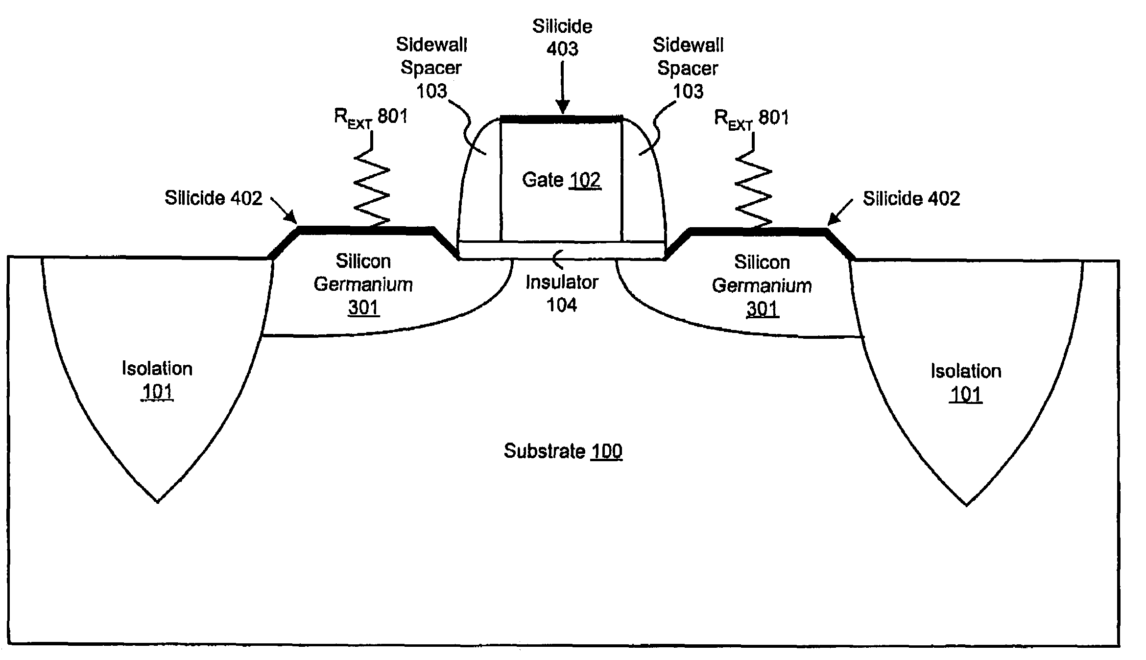
[0022]An embodiment of the invention reduces the external resistance of a transistor by utilizing a silicon germanium alloy for the source and drain regions and a nickel silicon germanium self-aligned silicide (i.e., salicide) layer to form the contact surface of the source and drain regions. The interface of the silicon germanium and the nickel silicon germanium silicide has a lower specific contact resistivity based on a decreased metal-semiconductor work function between th...


PUM


Abstract

An embodiment of the invention reduces the external resistance of a transistor by utilizing a silicon germanium alloy for the source and drain regions and a nickel silicon germanium self-aligned silicide (i.e., salicide) layer to form the contact surface of the source and drain regions. The interface of the silicon germanium and the nickel silicon germanium silicide has a lower specific contact resistivity based on a decreased metal-semiconductor work function between the silicon germanium and the silicide and the increased carrier mobility in silicon germanium versus silicon. The silicon germanium may be doped to further tune its electrical properties. A reduction of the external resistance of a transistor equates to increased transistor performance both in switching speed and power consumption.

Description

RELATED CASES[0001]This application is a divisional application of application Ser. No. 10 / 731,269 filed Dec. 8, 2003, now U.S. Pat. No. 6,949,482.FIELD[0002]Embodiments of the invention relate to high speed semiconductor transistors, and more specifically to increasing transistor performance by utilizing silicon germanium and improved methods of application thereof.BACKGROUND[0003]Silicon complementary metal oxide semiconductor (“CMOS”) technology is a dominant microelectronic technology. CMOS offers high reliability, high levels of integration, low power dissipation, and is very cost-effective. For lower frequency applications CMOS will most likely remain the dominant technology. However, electron and hole mobility in silicon limits the extent to which CMOS devices can be utilized for higher speed applications such as radars and mobile communication devices that require high transistor switching rates.[0004]One historical solution has been to use semiconductor compounds instead of...

Claims


Application Information

Patent Timeline
IPC IPC(8): H01L29/76H01L29/94H01L31/062H01L31/113H01L31/119H01L21/285H01L21/336H01L29/78
CPCH01L21/28518H01L29/165H01L29/665H01L29/6653H01L29/6656H01L29/66628H01L29/66636H01L29/78H01L29/7842H01L29/7848Y10S438/933H01L21/823814H01L29/6659H01L29/7833H01L21/823807H01L29/0653H01L29/0847H01L29/167H01L29/36H01L29/41725H01L29/6628
Inventor MURTHY, ANANDBOYANOV, BOYANGLASS, GLENN A.HOFFMANN, THOMAS
Owner INTEL CORP
Why Eureka
Try Eureka