Techniques for spin-flop switching with offset field

a technology of offset field and spin-flop, which is applied in the direction of spin-exchange-coupled multilayers, magnetic bodies, substrate/intermediate layers, etc., can solve the problem of low operating power, soft error rate due to thermally activated switching, and unintentional orientation change of magnetization of one or more magnetic memory cells. to achieve the effect of reducing the switching field

Inactive Publication Date: 2007-09-25
GOOGLE LLC
View PDF2 Cites 57 Cited by
  • Summary
  • Abstract
  • Description
  • Claims
  • Application Information

AI Technical Summary

Problems solved by technology

Unfortunately, in practice, the magnetization of one or more magnetic memory cells may change orientation unintentionally, due, at least in part, to thermal activation.
The resulting error rate due to thermally activated switching is called the soft error rate (SER).
Low operating power and small area requires a low switching field for the magnetic memory cell.
Therefore, as the area is scaled down, assuming nothing else changes, the activation energy barrier decreases and the SER becomes unacceptably large.
However, this technique is undesirable, at least in part because a greater magnetic field is required to switch the magnetization of a thicker cell.
However, while the techniques highlighted in Engel can be employed to reduce the write field, the effects of the offsetting field can result in an increased SER, potentially rendering the cell inoperable.

Method used


Image

  • Techniques for spin-flop switching with offset field
  • Techniques for spin-flop switching with offset field
  • Techniques for spin-flop switching with offset field

Examples


Embodiment Construction

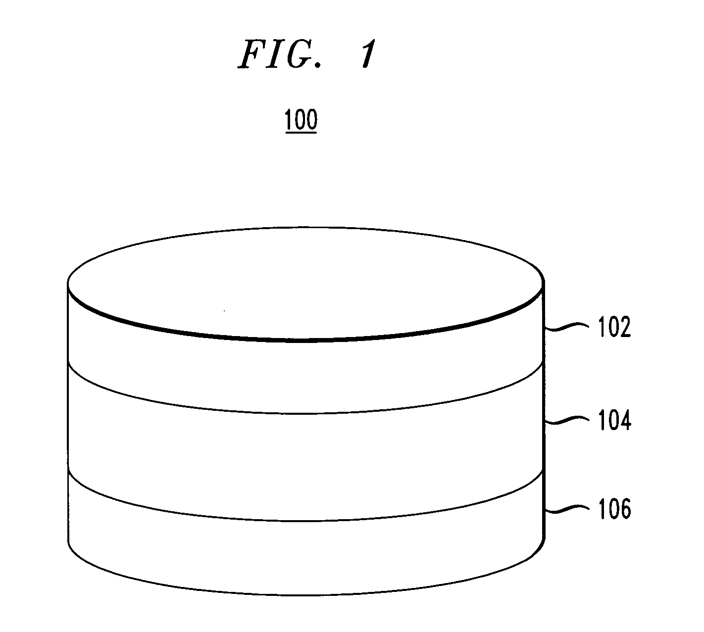
[0021]FIG. 1 is a diagram illustrating an exemplary semiconductor device 100. Semiconductor device 100, which may comprise a magnetic storage element in a magnetic random access memory (MRAM), comprises a first magnetic layer 102, spacer layer 104 and a second magnetic layer 106. Magnetic layers 102 and 106, as shown in FIG. 1, have a substantially elliptical shape. However, in accordance with the teachings presented herein, each of magnetic layers 102 and 106 may have any suitable non-elliptical shape, such as a substantially circular shape.

[0022]Each of magnetic layers 102 and 106 may comprise an element including, but not limited to, nickel, cobalt, iron, manganese and combinations comprising at least one of the foregoing elements. In an exemplary embodiment, first magnetic layer 102 and / or second magnetic layer 106 comprises Ni80Fe20. The composition of magnetic layer 102 may be the same as the composition of magnetic layer 106. Alternatively, the composition of magnetic layer 1...


PUM

PropertyMeasurementUnit
thicknessaaaaaaaaaa
thicknessaaaaaaaaaa
thicknessaaaaaaaaaa

Abstract

Techniques for reducing switching fields in semiconductor devices are provided. In one aspect, a semiconductor device comprising at least a first magnetic layer and a second magnetic layer with a spacer layer therebetween is provided. The semiconductor device is configured such that a thickness of at least one of the first magnetic layer and the second magnetic layer maintains a desired activation energy of the semiconductor device in the presence of an applied offsetting magnetic field. A method of reducing a switching field of a semiconductor device having at least a first magnetic layer and a second magnetic layer with a spacer layer therebetween is also provided.

Description

FIELD OF THE INVENTION[0001]The present invention relates to semiconductor devices and, more particularly, to reducing switching fields in semiconductor devices.BACKGROUND OF THE INVENTION[0002]Certain semiconductor devices, e.g., magnetic random access memory (MRAM) devices, use magnetic memory cells to store information. Each magnetic memory cell typically comprises a submicron piece of magnetic material, e.g., having the dimensions of 300 nanometers (nm) by 600 nm in area and five nm thick.[0003]Information is stored in such semiconductor devices as the orientation of the magnetization of a free layer in the magnetic memory cell as compared to the orientation of the magnetization of a fixed (e.g., reference) layer in the memory cell. The magnetization of the free layer may be oriented parallel or anti-parallel to the fixed layer, representing either a logic “1” or a “0.” The orientation of the magnetization of a given layer (fixed or free) may be represented by an arrow pointing ...

Claims


Application Information

Patent Timeline
Patent Type & Authority Patents(United States)
IPC IPC(8): H01L29/76H01F10/32H01L29/02H01L43/08
CPCB82Y25/00H01F10/3281H01L43/08H01F41/303H10N50/10
Inventor WORLEDGE, DANIEL C.
Owner GOOGLE LLC
Why Eureka
Try Eureka