Semiconductor device and manufacturing method thereof

a manufacturing method and technology for semiconductor devices, applied in manufacturing tools, welding/cutting media/materials, manufacturing tools, etc., can solve the problems of heat damage to be destroyed to increase the reactive surface, and print boards may be damaged. , to achieve the effect of increasing the reactive surfa

Inactive Publication Date: 2007-09-25
RENESAS ELECTRONICS CORP
View PDF5 Cites 4 Cited by
  • Summary
  • Abstract
  • Description
  • Claims
  • Application Information

AI Technical Summary

Benefits of technology

[0011]Therefore, an object of the present invention is to provide a manufacturing technology for semiconductor devices, which can reduce damage to the printed board by: specifying a material with a melting point of 260° C. or lower so as to be applied to the connection portion; providing the connection portion with a metal layer that reacts with the Pb-free solder at 260° C. or lower to form the compound with a melting point of 260° C. or higher; and thereby increasing the reactive interface.
[0014]The present invention is applied to a semiconductor device including a semiconductor element, a passive component, and a printed board having connected thereon the semiconductor element and the passive component, and to a semiconductor manufacturing method including a step of connecting a semiconductor element and a passive component onto a printed board through metal junction. In particular, at a connecting portion between the semiconductor element and the passive component, and the printed board, a material having a melting point not higher than 200° C., such as Sn, In, Sn—Ag base, Sn—Cu base, Sn—Ag—Cu base, Sn—Zn base, Sn—Zn—Bi base, Sn—In base, In—Ag base, In—Cu base, Bi—Sn base, or Bi—In base, is applied as a material having a melting point not higher than 260° C. Also, the connecting portion is provided with a metal layer of, for example, Cu, Ag, Ni, or Au, that reacts with a Pb-free solder having a melting point not higher than 260 degree Celsius to form an intermetallic compound having a melting point not lower than 260° C., thereby increasing a reactive surface.

Problems solved by technology

However, the techniques described in these two non-patent documents do not take the following points into consideration.
If the semiconductor element and the passive component are connected onto the printed board under such conditions, the printed board may be damaged by heat to be destroyed.

Method used


Image

  • Semiconductor device and manufacturing method thereof
  • Semiconductor device and manufacturing method thereof
  • Semiconductor device and manufacturing method thereof

Examples


first embodiment

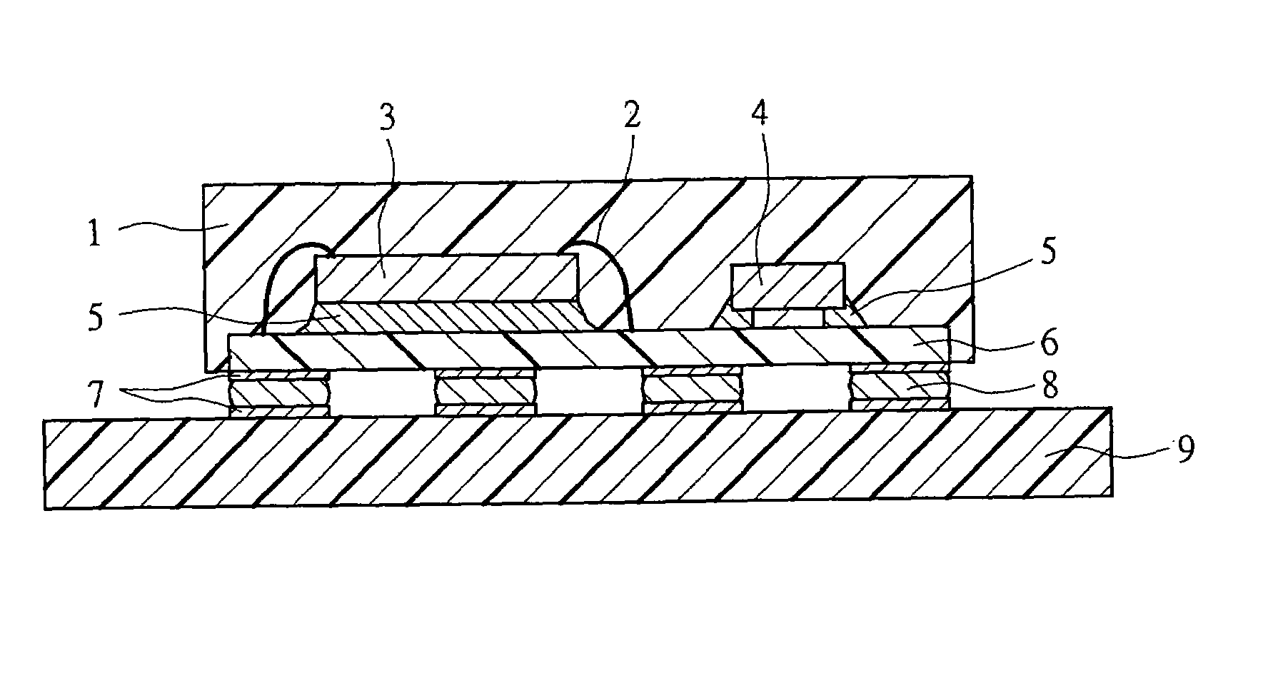
[0049]FIG. 8 shows a sectional view of a semiconductor device according to a first embodiment of the present invention.

[0050]The semiconductor device according to the present embodiment is applied to, for example, a power semiconductor module, and comprises a semiconductor element 3, a passive element (passive component) 4, a printed board (module board) 6a connecting the semiconductor element 3 and the passive element 4, wires 2 for wire-bonding between an electrode of the semiconductor element 3 and an electrode of the printed board 6a, and a mold resin 1 for sealing the semiconductor module, etc. This semiconductor module is mounted on the printed board 9, thereby being incorporated in various devices.

[0051]The process of manufacturing this semiconductor module will be described below. For example, when the internal connection of the semiconductor module is made by a structure of the connecting portion 17 of FIG. 7 as described above, a layer of a high-melting metal 20 and a laye...

second embodiment

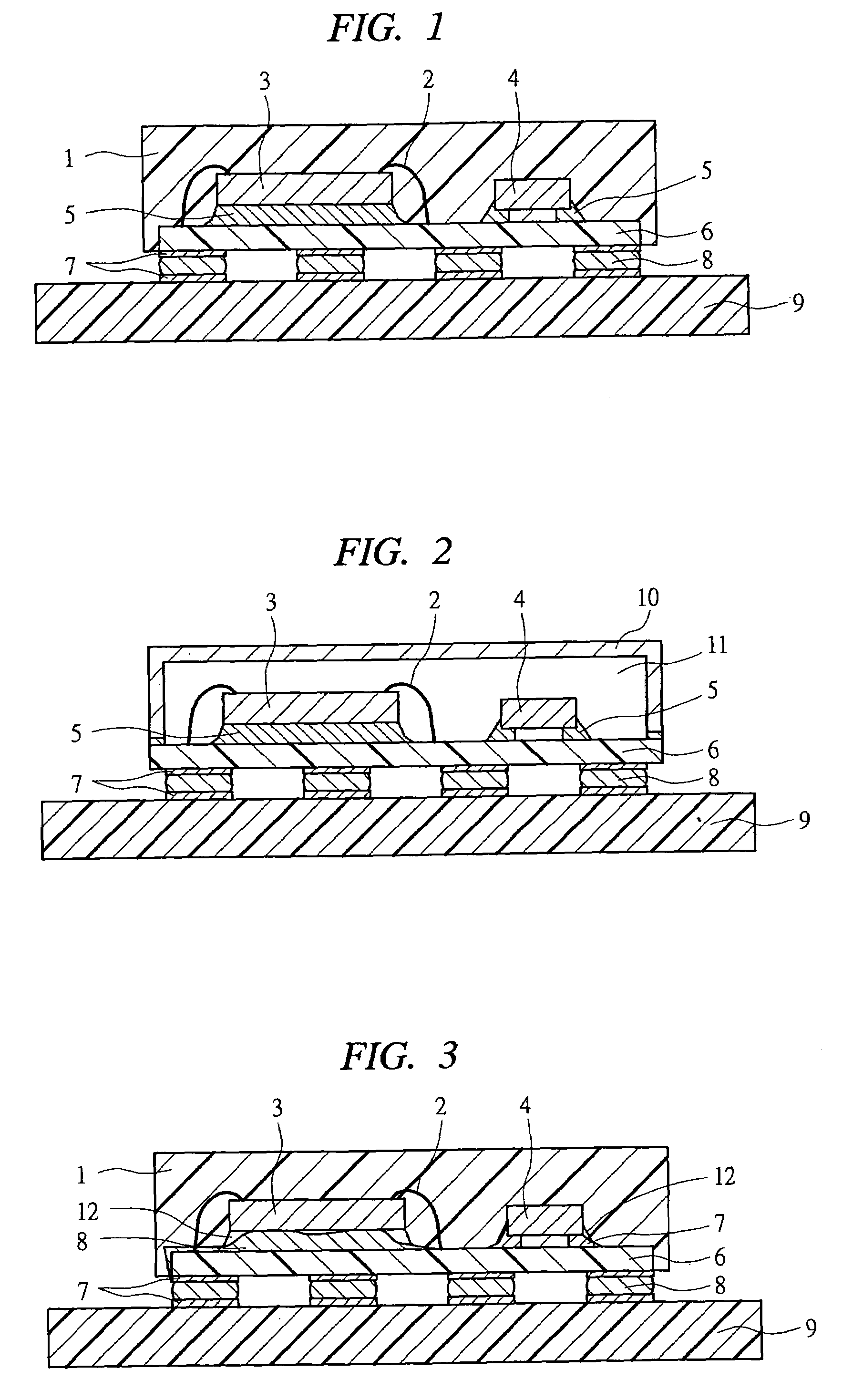
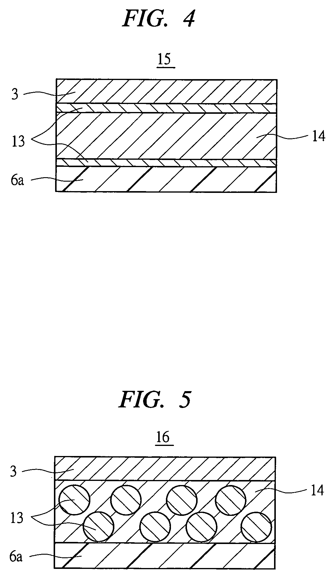
[0058]A semiconductor device according to a second embodiment of the present invention has the same constitution as that shown in the sectional view of FIG. 8 as described in the first embodiment but is different from it in that the structure of the above-described connection portion 15 in FIG. 4 is applied to the internal connection of the semiconductor module. Note that the case where the above-described structure of the connection portion 16 in FIG. 5 is applied is also the same.

[0059]A process of manufacturing this semiconductor module will be described below. When the internal connection of the semiconductor module is carried out by the above-described structure of the connection portion 15 in FIG. 4, a compound foil 30 shown in FIG. 12 is supplied onto the printed board 6a. This compound foil 30 is produced by providing, on surfaces of a layer of a high-melting metal 14, layers of low-melting solder 21 made of Pb-free solder with a melting point of 260° C. or lower. If the hig...


PUM

PropertyMeasurementUnit
melting pointaaaaaaaaaa
thicknessesaaaaaaaaaa
melting pointaaaaaaaaaa

Abstract

In a semiconductor module connecting a semiconductor element and a passive element to a printed board, each of connection portions between the semiconductor element and the printed board and between the passive element and the printed board includes a metal with a melting point of 260° C. or higher and an intermetallic compound with a melting point of 260° C. or higher. Specifically, by connecting them using Pb-free solder with a melting point of 260° C. or lower, the printed board capable of lowering in cost, lightening, and reducing back height can be applied to a module board.

Description

CROSS-REFERENCE TO RELATED APPLICATION[0001]The present application claims priority from Japanese patent application No. JP 2005-048808 filed on Feb. 24, 2005, the content of which is hereby incorporated by reference into this application.BACKGROUND OF THE INVENTION[0002]The present invention relates to a manufacturing technique for semiconductor devices and, particularly, to a technique effectively applied to a semiconductor module, in which a semiconductor element and a passive component are connected to a printed board by an intermetallic compound containing “no lead” (hereinafter referred to as “Pb-free”), and to a manufacturing method of the same.[0003]Regarding conventional semiconductor modules, the following techniques have been considered by the inventors.[0004]FIGS. 1 and 2 show sectional views semiconductor modules in the form of conventional structures. A semiconductor element 3 and a passive element 4 are connected onto a module board 6. After wire-bonding by wires 2, t...

Claims


Application Information

Patent Timeline
Patent Type & Authority Patents(United States)
IPC IPC(8): H01L23/52
CPCB23K35/0238B23K35/264H01L24/29H01L24/33H01L24/40H01L24/48H01L24/83H05K3/3463B23K35/262H01L2924/15747B23K2201/40H01L23/3128H01L2224/29109H01L2224/29111H01L2224/32507H01L2224/48091H01L2224/48227H01L2224/484H01L2224/73265H01L2224/83194H01L2224/83801H01L2224/8382H01L2224/83825H01L2924/01004H01L2924/01012H01L2924/01013H01L2924/01014H01L2924/01015H01L2924/01022H01L2924/01027H01L2924/01028H01L2924/01029H01L2924/0103H01L2924/01033H01L2924/01042H01L2924/01046H01L2924/01047H01L2924/0105H01L2924/01073H01L2924/01074H01L2924/01075H01L2924/01078H01L2924/01079H01L2924/01082H01L2924/01083H01L2924/01327H01L2924/014H01L2924/10329H01L2924/15311H01L2924/16152H01L2924/19105H01L2924/0132H01L2224/2919H01L2224/32225H01L2924/00014H01L2924/01006H01L2924/01024H01L2924/01044H01L2924/01087H01L2924/0665H01L2224/29101H01L2924/0133H01L2924/00H01L2924/00012H01L2224/45099H01L2924/01049H01L2924/3512H01L2224/83101H01L2924/351H01L2924/15787H01L2924/181H01L2224/40225H01L24/73H01L2224/8381H01L2224/371H01L2224/84801H01L2224/3754H01L24/37B23K2101/40H01L2224/73221H01L2224/85399H01L2224/05599
Inventor IKEDA, OSAMUOKAMOTO, MASAHIDESATOU, YUKIHIRO
Owner RENESAS ELECTRONICS CORP
Why Eureka
Try Eureka