Active matrix display device

a display device and active matrix technology, applied in the field of display devices, can solve the problems of inability to achieve the above-mentioned operation, unstable capacitance, and unstable dynamic ratio register operation, and achieve stable dynamic ratioless shift registers and design tolerance in states

Inactive Publication Date: 2007-09-25
PANASONIC LIQUID CRYSTAL DISPLAY CO LTD +1
View PDF6 Cites 11 Cited by
  • Summary
  • Abstract
  • Description
  • Claims
  • Application Information

AI Technical Summary

Problems solved by technology

However, such a phenomenon is not essential in the explanation of the operation, and, hence, the phenomenon is ignored.
However, when the dynamic ratio register having such a constitution is formed by directly providing MIS transistors having semiconductor layers which are made of polycrystalline silicon (p-Si) to surfaces of substrates (glass substrates) which are arranged to face each other in an opposed manner through a liquid crystal, it has been confirmed that the dynamic ratio register operates in an extremely unstable manner, so that a countermeasure to cope with such a phenomenon is needed.
However, when a similar circuit made of monocrystalline thin film transistors is formed on a glass substrate, the above-mentioned operation is not achieved.
This capacitance becomes a cause of instability.
That is, an unstable operation is generated such that nodes which are irrelevant to the node under control become “H” and generate outputs or start the scanning from such portions.

Method used


Image

  • Active matrix display device
  • Active matrix display device
  • Active matrix display device

Examples


embodiment 2

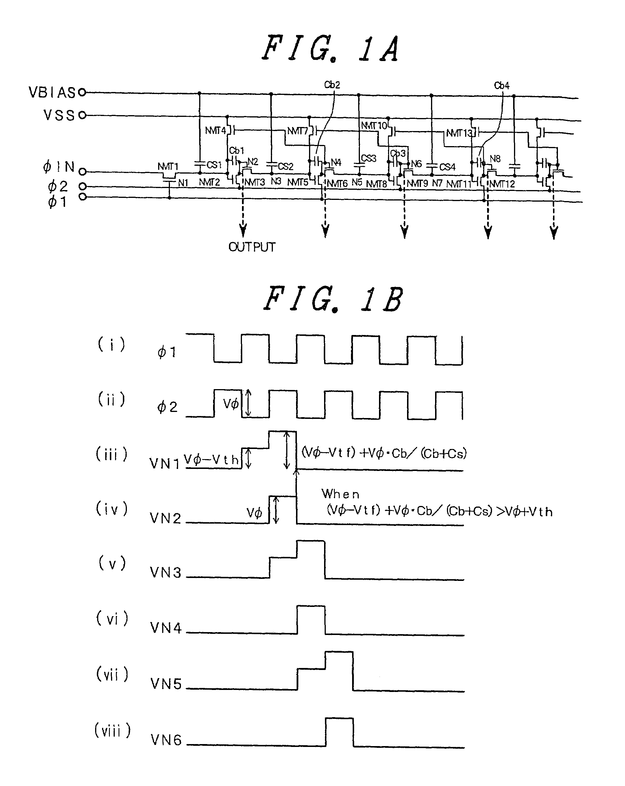
[0106]FIG. 6A is a circuit diagram which shows another embodiment of a shift register formed in a liquid crystal display device according to the present invention. This embodiment is constituted differently from the embodiment 1 in which the OFF level is held by adding the load capacitance. That is, this embodiment is constituted such that a circuit is added which changes an input gate of a shift register which is not selected to “L”. That is, as shown in FIG. 6A, first of all, aMOS transistor NMT1 has the first terminal and a gate terminal thereof connected to an input terminal of an input pulse φIN thus forming an inputting part.

[0107]The MOS transistor NMT1 has the second terminal thereof connected to a gate terminal of a MOS transistor NMT4 and the first terminal of a MOS transistor NMT2. Further, the second terminal of the MOS transistor NMT1 is connected to the first terminal of a capacitance element CB1. The second terminal of a capacitance element CB2 is connected to the sec...

embodiment 3

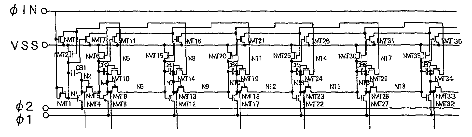
[0129]FIG. 7A is a circuit diagram which shows another embodiment of the shift register formed on the liquid crystal display device of the present invention.

[0130]In the drawing, a circuit is constituted such that thin film transistors NNTR1, NMTR2, NNTR3, . . . which are subjected to the diode connection using respective nodes N11, N14, N17, as sources thereof and the input pulse signal φIN as drains and gates thereof are connected to the circuit exemplified in the embodiment 2.

[0131]These respective thin film transistors NMTR1, NNTR2, NMTR3, . . . reinforce the “H” level of respective nodes in the floating state when the input pulse signal φIN becomes the “H” state, thus making the forced OFF state of the non-selected input gate more reliable.

[0132]Further, an advantageous effect is obtained in that, at the start of scanning immediately after the supply of electricity, an initialization equal to that of the normal operating state can be performed.

[0133]Although the thin film trans...

embodiment 4

[0135]FIG. 11 is a circuit diagram showing another embodiment of a ratioless-type dynamic shift register which is used in the display device of the present invention. That is, this embodiment shows a further improvement of the dynamic shift registers shown in the above-mentioned respective embodiments. Further, FIG. 12 shows an input pulse timing chart of the circuit shown in FIG. 11.

[0136]Here, to clarify the characterizing portion of the ratioless-type dynamic shift register which is used in the display device of the present invention, a circuit diagram which is used for comparison is shown in FIG. 13. Further, FIG. 14 shows an input pulse timing chart of the circuit shown in FIG. 13.

[0137]In such a circuit, a jumping of the H1 clock is observed at a VSS (GND) level of a node 3 in FIG. 13. FIG. 15A illustrates this phenomenon, wherein an H1 clock after an input signal Hin appears at the VSS (GND) level (lower side of the drawing) of the node 3.

[0138]Due to a pulse which enters a n...


PUM

PropertyMeasurementUnit
voltageaaaaaaaaaa
fixed voltageaaaaaaaaaa
electric fieldaaaaaaaaaa

Abstract

A display device includes a dynamic ratioless shift register which is operated in a stable manner and can expand the degree of freedom of design. In the dynamic ratioless shift register which is provided with thin film transistors having semiconductor layers made of p-Si on a substrate surface, a node which becomes the floating state is connected to a fixed potential through a capacitance element.

Description

CROSS-REFERENCE TO RELATED APPLICATIONS[0001]This application is a Continuation application of Ser. No. 09 / 981,804, filed Oct. 19, 2001 now U.S. Pat. No. 6,801,194, the entire disclosure of which is hereby incorporated by reference.BACKGROUND OF THE INVENTION[0002]The present invention relates to a display device, and, more particularly, to an active matrix type display device thereof.[0003]In an active matrix type liquid crystal display device, pixel regions are formed on a liquid crystal side surface of one of a pair of substrates, which are arranged so as to face each other in an opposed manner, with a liquid crystal being disposed therebetween. The pixels are formed as regions which are surrounded by gate signal lines that extend in the x direction and are arranged in parallel in the y direction and drain signal lines that extend in the y direction and are arranged in parallel in the x direction.[0004]Each pixel region is provided with a thin film transistor, which is operated u...

Claims


Application Information

Patent Timeline
Patent Type & Authority Patents(United States)
IPC IPC(8): G09G5/00G02F1/1368G02F1/133G09G3/20G09G3/36G09G5/39G11C19/00H01L27/12H01L29/423H03K5/15H03K23/54
CPCG09G3/3677G09G3/3648H01L27/12H01L29/42384G09G3/36G11C19/184G09G5/39G09G2300/0408G09G2330/021G09G3/3696G02F1/133G09G3/3659G09G3/3688G09G2310/0286G09G2310/08G11C19/28H01L27/124
Inventor MIYAZAWA, TOSHIOTAKEMOTO, IWAOHASEGAWA, ATSUSHIMAKI, MASASHIROGOTO, KAZUTAKA
Owner PANASONIC LIQUID CRYSTAL DISPLAY CO LTD
Why Eureka
Try Eureka