LED lamp

a technology of led lamps and diodes, which is applied in the direction of sustainable manufacturing/processing, light source combinations, and final product manufacturing, etc., can solve the problems of difficult stably secure electrical connections, difficult to mount led workability, and complicated manufacturing processes, and achieve easy acquisition of enhanced solder bonding properties.

Inactive Publication Date: 2007-10-09
TOYODA GOSEI CO LTD +1
View PDF7 Cites 45 Cited by
  • Summary
  • Abstract
  • Description
  • Claims
  • Application Information

AI Technical Summary

Benefits of technology

[0038]In this composition, with the cutting region, a suitable amount of solder can be supplied to the connection part of the terminal of package and the wiring pattern of circuit board. Therefore, the enhanced solder bonding property can be obtained easily.

Problems solved by technology

On the other hand, the mounting workability of LED becomes serious according as the LED lamp is downsized.
Namely, since the mounting area decreases as LED lamp is downsized, it is difficult to stably secure the electrical connection while securing a sufficient bonding strength.
Therefore, the manufacturing process must be complicated.

Method used


Image

  • LED lamp
  • LED lamp
  • LED lamp

Examples


first embodiment

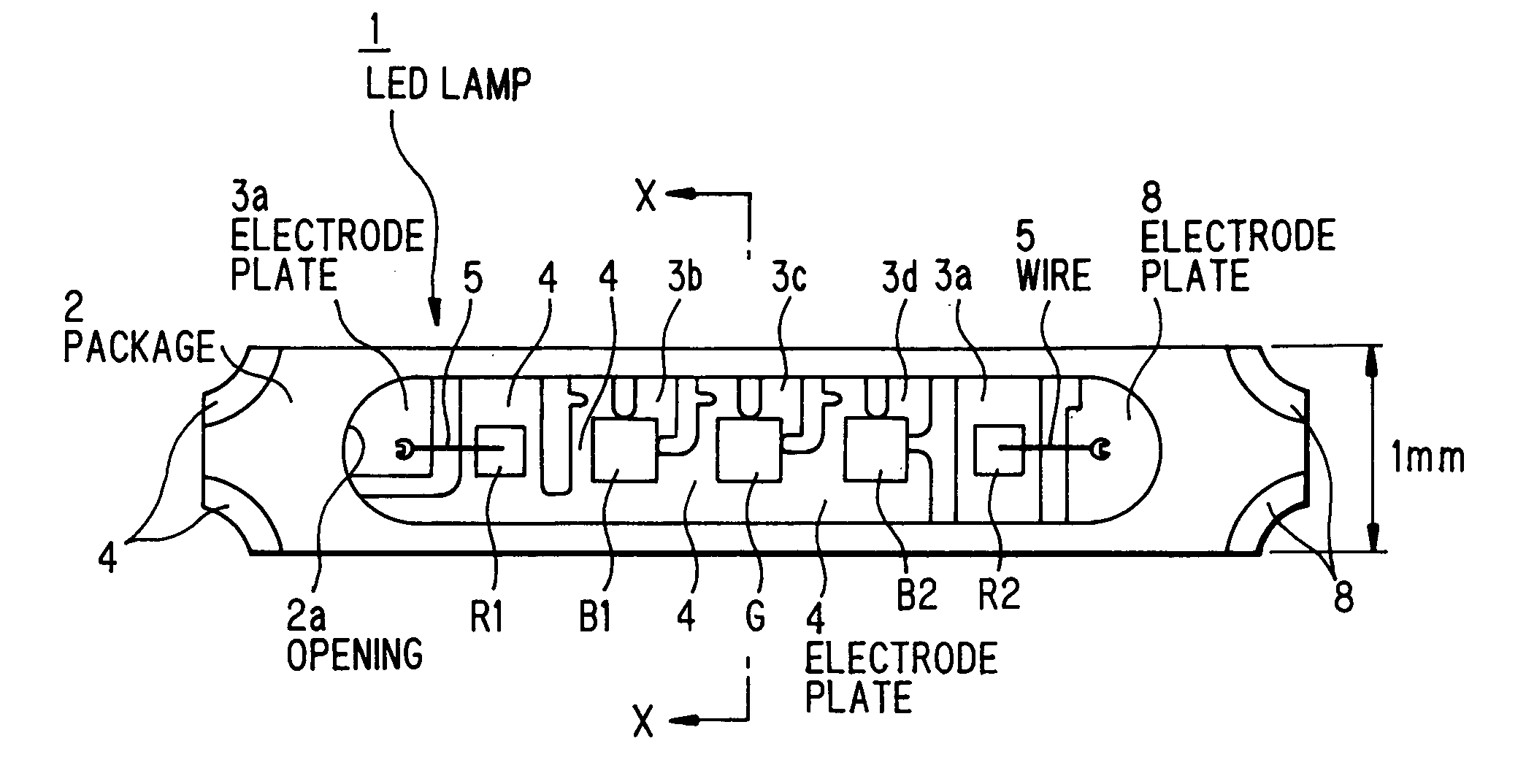
[0066]FIG. 3A is a plain view showing an LED lamp 1 in the first embodiment of the invention. FIG. 3B is a side view showing the LED lamp 1 in FIG. 3A. FIG. 3C is across sectional view cut along the line X-X in FIG. 3A.

[0067]As shown in FIG. 3A, the LED lamp 1 is provided with electrode plates 3a, 3b, 3c, 3d, 4 and 8 on the bottom surface of an opening 2a in a package 2 of alumina (Al2O3) that are insulated one another and part of which penetrates to the bottom surface (backsurface) of the package 2. At both ends, red light emitting elements R1, R2 are die bonded on the electrode plates 4, 3a. The upper-surface electrode (not shown) of red light emitting element R1 is bonded through a wire 5 to the electrode plate 3a at the left end. The upper-surface electrode (not shown) of red light emitting element R2 is bonded through a wire 5 to the electrode plate 8. Further, a conduction line (not shown) penetrates from the left-end electrode plate 3a to the right-end electrode plate 3a in t...

second embodiment

[0081]FIG. 7 is a front view showing an LED lamp 101 in the second preferred embodiment of the invention. The LED lamp 101 is composed of: a package 102 that is formed by stacking thin plate members; LED's 103R1, 103R2, 103G, 103B1 and 103B2 that are housed in an opening 2a of the package 102; a wiring pattern 104 that is formed on a board as described later to offer the electrical connection to LED's; a sealing material 102B of transparent epoxy resin to be filled in the opening 102A to protect LED's.

[0082]The package 2 is formed by stacking a plurality of thin plate members of ceramics, and LED's 103R1, 103R2, 103G, 103B1 and 103B2 are arrayed in the ellipse-shaped opening 2A to compose the LED lamp. The package 102 is provided with corners 102a that are shaped like an inverted arc.

[0083]LED's 103R1, 103R2 each have electrodes on its top and bottom surfaces and the top electrode is electrically connected through a wire 105 to the wiring pattern 104. LED's 103G (green), 103B1 and 1...

third embodiment

[0112]FIG. 13A is a perspective view showing an LED lamp 101 in the third preferred embodiment of the invention. FIG. 13B is an enlarged perspective view showing a cutting region 107A in FIG. 13A. This perspective view is viewed from the bottom side opposite to the light emission surface of LED lamp 101 mounted on the external board 108. Like components are indicated by the same reference numerals used in the second embodiment.

[0113]In the third embodiment, the wiring patter 109 is provided with a groove 109A corresponding to the position of cutting region 107A. As shown in FIG. 13B, the groove 109A is disposed such that it has a deviation 1 to the cutting region 107A. The 109A is obtained by partially removing the wiring pattern 109A and external board 108 by, e.g., etching.

[0114]The effects of the third embodiment are as follows.[0115](i) With the groove 109A provided in the wiring pattern 109 corresponding to the cutting region 107A, the number of edges to promote the flowing of ...


PUM

PropertyMeasurementUnit
heightaaaaaaaaaa
heightaaaaaaaaaa
thicknessaaaaaaaaaa

Abstract

An LED lamp has a package and a plurality of light emitting elements that are electrically connected to a plurality of electrode plates provided in the package and that are sealed with transparent material. A red light emitting element of the plurality of light emitting elements is wire bonded along the longitudinal direction of the package, a green light emitting element and a blue light emitting element are flip-chip bonded with its electrode faced down, and the electrodes are extended to a surface opposite to the light emission surface of the LED lamp while being embedded in the package.

Description

[0001]The present application is based on Japanese patent application Nos. 2003-078267 and 2003-288294, the entire contents of which are incorporated herein by reference.BACKGROUND OF THE INVENTION[0002]1. Field of the Invention[0003]The invention relates to a light emitting diode lamp (herein referred to as an LED lamp) and, particularly, to an LED lamp that a plurality of light emitting elements, and electrode plates and wires for electrical connection with these light emitting elements are housed in a package of a material such as ceramics and are sealed with transparent epoxy resin.[0004]Also, the invention relates to an LED lamp that is intended to have stable solder connectivity when being connected with a wiring pattern.[0005]Herein, an LED chip itself is referred to as a light emitting element or light emitting diode (LED), and a whole structure with a plurality of LED chips is referred to as a light emitting diode lamp or LED lamp.[0006]2. Description of the Related Art[000...

Claims


Application Information

Patent Timeline
Patent Type & Authority Patents(United States)
IPC IPC(8): H01L29/24H01L29/18H01L33/00F21K99/00H01L25/075
CPCF21K99/00H01L25/0753H05K3/3442H05K3/366H05K2201/09181H01L2224/48091H05K2201/10106H01L2924/00014F21K9/00F21Y2113/13F21Y2115/10Y02P70/50
Inventor MATSUMURA, KANAEKATO, HIDEAKITESHIMA, KIYOTAKAOHTSUKA, SHUNSUKE
Owner TOYODA GOSEI CO LTD
Why Eureka
Try Eureka