
Method for fabricating a film bulk acoustic resonator

a resonator and film technology, applied in the direction of generator/motor, device details, device material selection, etc., can solve the problems of increasing the manufacturing cost, difficult membrane fabrication, and precise thickness control of the reflection structure layer , so as to prevent the damage of the fbar, enhance the q-value of the fbar, and simplify the fbar fabrication.

Active Publication Date: 2007-10-16
SAMSUNG ELECTRONICS CO LTD
View PDF27 Cites 56 Cited by
  • Summary
  • Abstract
  • Description
  • Claims
  • Application Information

AI Technical Summary

Benefits of technology

[0011]It is a feature of the present invention to provide a simpler FBAR fabrication. It is another feature of the present invention to prevent a FBAR from being damaged during fabrication. It is yet another feature of the present invention to enhance the Q-value of the FBAR. It is further another feature of the present invention to simplify connection of the electrodes of the FBAR with external terminals.

Problems solved by technology

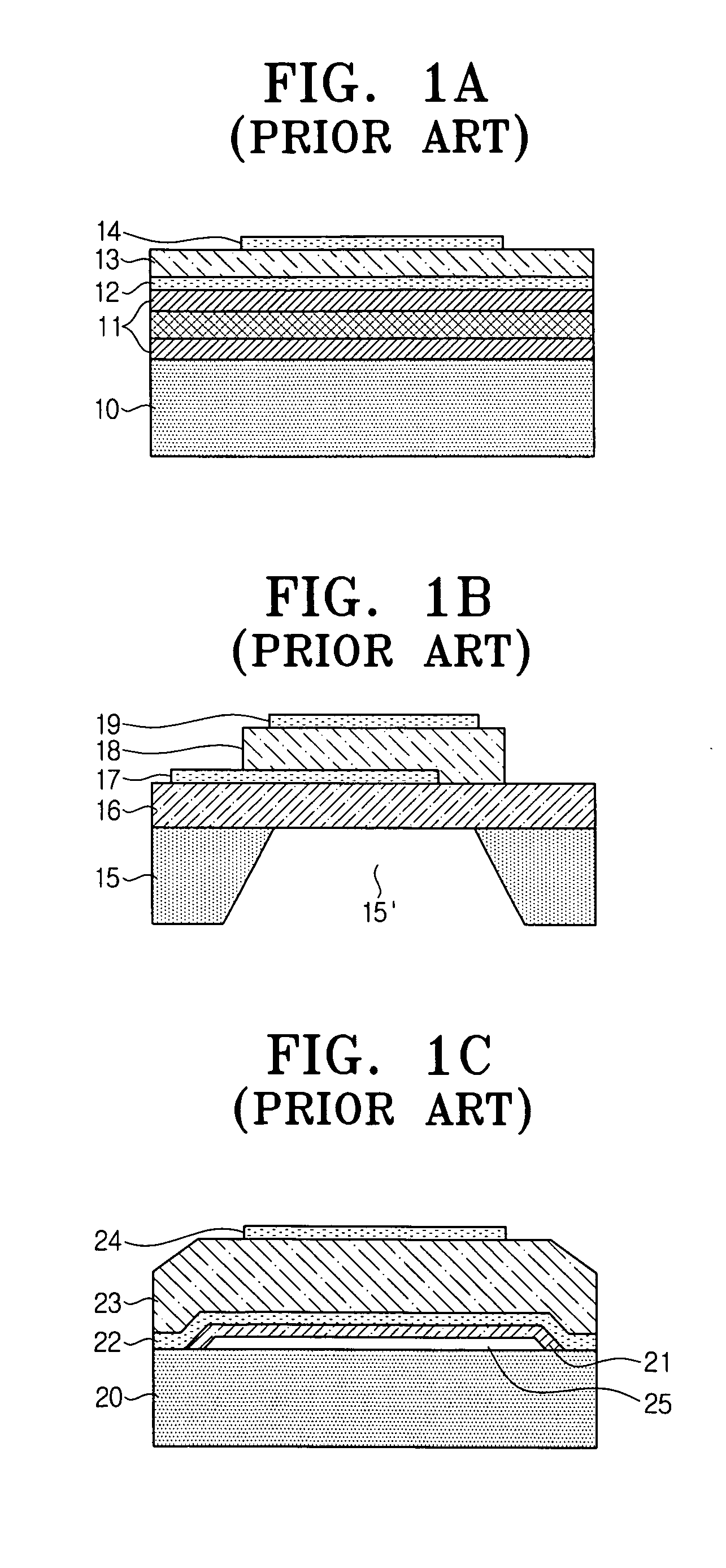
However, the precise thickness control of the layers of the reflection structure 11 for the total reflection in such a Bragg reflector type FBAR is not easy and increases the manufacturing cost.
However, the fabrication of the membrane is difficult and the devices are frequently damaged during the etching process of substrates thereof.
However, this fabrication process is complicated, and collapse and peeling off of the structure may result during the process.
However, this fabrication process is complicated because the process includes laminating and patterning the SiO2 layer.
It is difficult to precisely control the resistance of these connections.
Also, the separate connection required for each FBAR do not facilitate using a plurality of FBARs to form a more complex structure, such as a filter.

Method used


Image

  • Method for fabricating a film bulk acoustic resonator
  • Method for fabricating a film bulk acoustic resonator
  • Method for fabricating a film bulk acoustic resonator

Examples


first embodiment

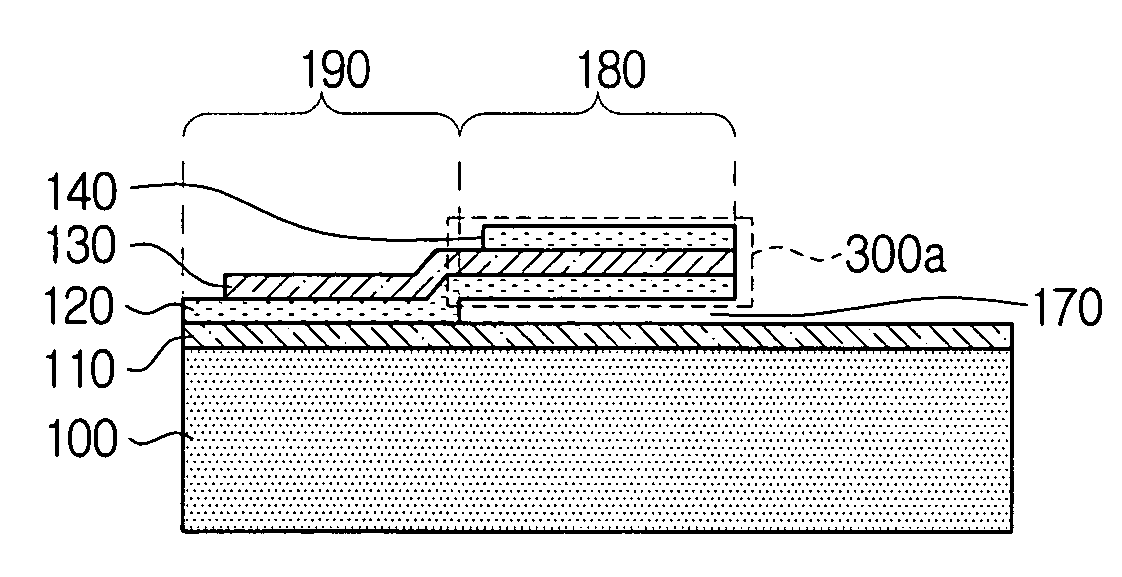
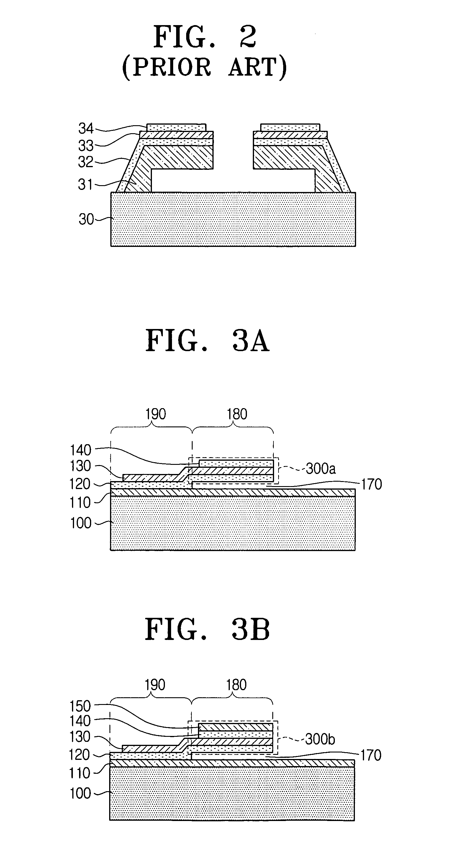
[0034]FIGS. 3A and 3B show the final structure of the cantilevered type FBARs fabricated according to the present invention. FIGS. 4A to 4F show the respective steps of the process for fabricating such a cantilevered type FBAR. The FBAR of FIG. 3B requires the additional step shown in FIG. 4G.

[0035]First, as shown in FIG. 4A, a dielectric layer 110 is deposited on a substrate 100. The dielectric layer 110 serves to isolate the substrate 100 and an electrode layer 120 from each other and to facilitate the deposition of the electrode layer 120. The substrate 100 may be a typical silicone wafer, e.g., a high resistance silicon (HRS) substrate. The dielectric layer 110 may be, for example, silicone oxide (SiO2) or aluminum oxide (Al2O2).

[0036]Next, as shown in FIG. 4B a sacrificial layer 160 is deposited and patterned on the dielectric layer 110. Through the patterning, the sacrificial layer 160 is removed or is otherwise not present in the area where the bottom electrode 120 will adjoi...

second embodiment

[0056]FIGS. 5A and 5B illustrate the final structures of the cantilevered type FBAR fabricated according to the present invention. The FBAR has a cavity 270 at a predetermined area of the substrate 200, and a dielectric layer 210a, 210, 210b on the substrate having the cavity 270. The bottom electrode 220 overlaps the part 210a of the dielectric layer, thereby forming a base section 290. The bottom electrode 220 extends over the cavity 270, thereby forming an overhanging section 280. The piezoelectric layer 230 is provided over the entire overhanging section 280 and over part of the base section 290. The top electrode 240 is provided on the piezoelectric layer 230 on the overhanging section 280, thereby forming a resonance section 400a.

[0057]The FBAR shown in FIG. 5B has an additional dielectric layer 250 deposited on the top electrode 240, thereby reinforcing the rigidity of a resonance section 400b. The thickness of the second dielectric layer 250 on the resonance section 400b ma...

third embodiment

[0059]According to the present invention, as shown in FIG. 7A, after depositing the bottom electrode 120 on the sacrificial layer 160 and the dielectric layer 110, as shown in FIG. 4C, a part of the bottom electrode 120 forming the base section 190 is removed so that the width l1 of the bottom electrode 120 forming the base section 190 is smaller than the width l2 of the bottom electrode 120 forming the overhanging section 180. After depositing the top electrode 140 on the piezoelectric layer 130, as shown in FIG. 4E, the top electrode 140 is patterned so that the top electrode 140 is positioned in the area of the dielectric layer 110, where the bottom electrode has been removed, and spaced from the part of the bottom electrode 120 left in the base section 190. Thus, pads 500a, 500b for connecting the top and bottom electrodes with external terminals, respectively, may be formed.

[0060]As shown in FIG. 7A, in creating the pads 500a, 500b, the piezoelectric layer 130 no longer extends...


PUM

PropertyMeasurementUnit
depthaaaaaaaaaa
conductiveaaaaaaaaaa
dielectricaaaaaaaaaa

Abstract

A method for fabricating a film bulk acoustic resonator (FBAR) includes depositing a dielectric layer on a substrate, providing a sacrificial layer on part of the dielectric layer; providing a bottom electrode on part of the sacrificial layer on part of the dielectric layer; providing a piezoelectric layer on the bottom electrode; patterning a top electrode on the piezoelectric layer; and removing the sacrificial layer. The substrate may have a cavity receiving the sacrificial layer. As a result, a cantilevered resonator having an air gap between the bottom electrode and the dielectric layer may be simply fabricated.

Description

BACKGROUND OF THE INVENTION[0001]1. Field of the Invention[0002]The present invention relates to a method for fabricating a cantilevered type film bulk acoustic resonator and a film bulk acoustic resonator fabricated by the method.[0003]2. Description of the Related Art[0004]As mobile communication devices, such as portable telephones, become increasingly prevalent, demand for compact, lightweight filters used in such devices is also rising. Film bulk acoustic resonators (FBARs) can be used as such compact, lightweight filters. FBARs can be inexpensively mass-produced and can be implemented in a micro-structure. A FBAR has a multi-layer resonance section in which a bottom electrode, a piezoelectric layer, and a top electrode are sequentially provided in this order. The FBAR uses a piezoelectric phenomenon, by which when electric energy is applied to the top and bottom electrodes, piezoelectric effect is produced and resonance results. In such a FBAR, separation between the substrate...

Claims


Application Information

Patent Timeline
Patent Type & Authority Patents(United States)
IPC IPC(8): H04R17/00H01L41/00H01L41/09H01L41/02H01L41/08H01L41/18H01L41/187H01L41/22H01L41/23H01L41/253H03H3/02H03H3/04H03H9/17
CPCH03H3/02H03H9/172H03H2003/022Y10T29/4913Y10T29/49156Y10T29/49128Y10T29/49155Y10T29/49005Y10T29/49126Y10T29/42H10N30/80
Inventor KIM, SANG-CHAESONG, IN-SANGHONG, YOUNG-TACK
Owner SAMSUNG ELECTRONICS CO LTD
Learn More